Until recently, it was widely believed among physicists that it was impossible to compress light below the so-called diffraction limit (see below), except when using metal nanoparticles, which unfortunately also absorb light. It therefore seemed impossible to compress light strongly in dielectric materials such as silicon, which are key materials in information technologies and come with the important advantage that they do not absorb light.
Interestingly, it was shown theoretically in 2006 that the diffraction limit also does not apply to dielectrics. Still, no one has succeeded in showing this in the real world, simply because no one has been able to build the necessary dielectric nanostructures until now.
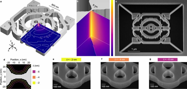
A research team from DTU has successfully designed and built a structure, a so-called dielectric nanocavity, which concentrates light in a volume 12 times below the diffraction limit. The result is groundbreaking in optical research and has just been published in Nature Communications.
“Although computer calculations show that you can concentrate light at an infinitely small point, this only applies in theory. The actual results are limited by how small details can be made, for example, on a microchip,” says Marcus Albrechtsen, Ph.D.-student at DTU Electro and first author of the new article.
“We programmed our knowledge of real photonic nanotechnology and its current limitations into a computer. Then we asked the computer to find a pattern that collects the photons in an unprecedentedly small area—in an optical nanocavity—which we were also able to build in the laboratory.”
Optical nanocavities are structures specially designed to retain light so that it does not propagate as we are used to but is thrown back and forth as if you put two mirrors facing each other. The closer you place the mirrors to each other, the more intense the light between the mirrors becomes. For this experiment, the researchers have designed a so-called bowtie structure, which is particularly effective at squeezing the photons together due to its special shape.
The nanocavity is made of silicon, the dielectric material on which most advanced modern technology is based. The material for the nanocavity was developed in cleanroom laboratories at DTU, and the patterns on which the cavity is based are optimized and designed using a unique method for topology optimization developed at DTU. Initially developed to design bridges and aircraft wings, it is now also used for nanophotonic structures.
“It required a great joint effort to achieve this breakthrough. It has only been possible because we have managed to combine world-leading research from several research groups at DTU,” says associate professor Søren Stobbe, who has led the research work.”
Important breakthrough for energy-efficient technology
The discovery could be decisive for developing revolutionary new technologies that may reduce the amount of energy-guzzling components in data centers, computers, telephones, and so on.
The energy consumption for computers and data centers continues to grow, and there is a need for more sustainable chip architectures that use less energy. This can be achieved by replacing the electrical circuits with optical components. The researchers’ vision is to use the same division of labor between light and electrons used for the Internet, where light is used for communication and electronics for data processing. The only difference is that both functionalities must be built into the same chip, which requires that the light be compressed to the same size as the electronic components. The breakthrough at DTU shows that it is, in fact, possible.
“There is no doubt that this is an important step to developing a more energy-efficient technology for, e.g., nanolasers for optical connections in data centers and future computers—but there is still a long way to go,” says Marcus Albrechtsen.
The researchers will now work further and refine methods and materials to find the optimal solution.
“Now that we have the theory and method in place, we will be able to make increasingly intense photons as the surrounding technology develops. I am convinced that this is just the first of a long series of major developments in physics and photonic nanotechnology centered around these principles,” says Søren Stobbe.
The diffraction limit
The theory of the diffraction limit describes that light cannot be focused to a volume smaller than half the wavelength in an optical system—for example, this applies to the resolution in microscopes.
However, nanostructures can consist of elements much smaller than the wavelength, which means that the diffraction limit is no longer a fundamental limit. Bowtie structures, in particular, can compress the light into very small volumes limited by the sizes of the bowtie and, thus, the quality of the nanofabrication.

When the light is compressed, it becomes more intense, enhancing interactions between light and materials such as atoms, molecules and 2D materials.
Dielectric materials
Dielectric materials are electrically insulating. Glass, rubber, and plastic are examples of dielectric materials, and they contrast with metals, which are electrically conductive.
An example of a dielectric material is silicon, which is often used in electronics but also photonics.
More information:
Marcus Albrechtsen et al, Nanometer-scale photon confinement in topology-optimized dielectric cavities, Nature Communications (2022). DOI: 10.1038/s41467-022-33874-w
Provided by
Technical University of Denmark
Citation:
Researchers compress light 12 times below the diffraction limit in a dielectric material (2022, October 26)