Envision a realm where light can be meticulously controlled and manipulated at minuscule scales, unlocking unprecedented potentials for nanotechnology and quantum information technology. Recent breakthroughs in quantum research have propelled us closer to a reality that may be more achievable than previously realized.
In this article, we delve into the domain of surface plasmon polaritons (SPPs) and the vast possibilities they offer in revolutionizing the field of quantum optics.
Surface plasmon polaritons (SPPs)
Picture a serene lake on a sunny day. As you drop a small stone into the water, it sets in motion gentle ripples that traverse the surface. Now, imagine light as akin to those undulating ripples. When light encounters the interface of a metal and a dielectric material, it has the power to generate waves, much like the ripples on the lake. This phenomenon is even more intriguing because these light waves can interact with the metal’s microscopic constituents, such as electrons. Remarkably, the light waves and electrons synchronize their oscillations, giving rise to an SPP wave.
This new wave gracefully travels along the metal’s surface, reminiscent of the lake’s ripples but infused with the essence of light. SPPs possess exceptional traits, as they can navigate through minuscule gaps on the metal surface, akin to maneuvering through a labyrinth. Scientists dedicate their studies to SPPs due to their distinctive properties and capabilities beyond those of ordinary light waves. The capacity to traverse such tiny spaces facilitates the development of nanoscale electronic devices, including data processing units and sensors. These advancements pave the way for cutting-edge quantum technologies, promising a future of immense possibilities.
Schottky junction
Traditional SPPs, which occur at a metal and a dielectric material interface, have already demonstrated remarkable potential in nanophotonics. However, scientists have recently made an intriguing discovery that adds a new dimension to this phenomenon.
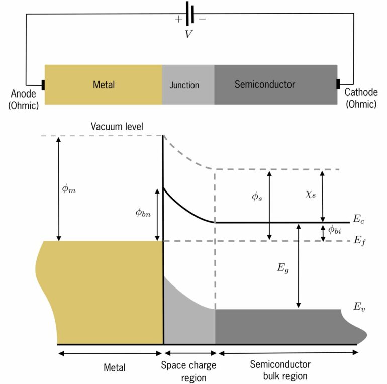
When metal and semiconductors combine to create a Schottky junction [Fig. 1], something extraordinary unfolds where a separate space charge region emerges at this junction due to the contrasting charge carrier densities between the metal and the semiconductor [1]. This region alters the interface’s properties, leading to transformations in the behavior of SPPs. It’s akin to unearthing an entirely novel wave at this exceptional interface.

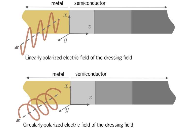
Figure 2. Within the Schottky junction, the metal region encounters two distinct types of incident light: a linearly polarized dressing field from the top and a circularly polarized dressing field from the bottom. Through a quantum description, we can demonstrate that this phenomenon enables us to actively manipulate the movement of surface plasmon polaritons (SPPs) along the interface. © Kosala Herath, Sarath D. Gunapala, and Malin Premaratne
Quantum description of the Schottky junction based dressed SPPs
Our research team has developed a comprehensive theoretical framework grounded in quantum theory [2] that enables accurate predictions of SPP behavior at the Schottky junction when subjected to an external electromagnetic field [Fig. 2]. We published our findings in Scientific Reports.
Through the application of quantum principles, we have derived an expression for the dielectric function of the “dressed” metal. But what exactly does “dressing” entail in this context? Recent scientific breakthroughs have revealed that an external electromagnetic field possesses the ability to “dress” or modify the properties of metals using Floquet engineering techniques [3,4,5]. It is essential to emphasize that these observations can only be comprehended and explained within the framework of quantum theory.
Now, here comes the truly exciting part: This dressing field provides a potent tool to control and enhance the propagation of SPPs. It alters the metal’s susceptibility and permittivity functions, thereby transforming its interaction with light and other electromagnetic waves. By adjusting the intensity, frequency and polarization of this external field, we can finely tune the mobility of electrons within the metal. Our findings have revealed that by doing so, we can extend the distance over which SPPs can travel without dissipating energy. This advancement holds crucial implications for the development of practical nanoscale data processing devices in real-world applications.
What implications does all of this hold for our world? Let your imagination soar as you envision a future where incredibly tiny circuits harness the power of light to fuel our devices. These circuits would exhibit exceptional efficiency and process information at astonishing speeds. This breakthrough in controlling and enhancing light propagation at the nanoscale opens up many possibilities for the future of quantum information technology.
The ability to meticulously control light waves paves the way for the development of advanced quantum photonic circuits and devices surpassing current electronic components’ capabilities. Picture smartphones that are faster, smaller and more powerful than ever before, effortlessly handling complex tasks. Envision rapid data processing and sharing systems that revolutionize telecommunications, computing, and health care industries.
With such advancements, the landscape of technology and various sectors would undergo profound transformations. These breakthroughs have the potential to reshape our world, enabling remarkable progress in communication, computation, and health care, to name just a few.
This story is part of Science X Dialog, where researchers can report findings from their published research articles. Visit this page for information about ScienceX Dialog and how to participate.
More information:
[1] Malin Premaratne and Govind P. Agrawal, Theoretical foundations of nanoscale quantum devices, Cambridge University Press (2021). DOI: 10.1017/9781108634472
[2] Kosala Herath et al, A Floquet engineering approach to optimize Schottky junction-based surface plasmonic waveguides, Scientific Reports (2023). DOI: 10.1038/s41598-023-37801-x
[3] Kosala Herath et al, Generalized model for the charge transport properties of dressed quantum Hall systems, Physical Review B (2022). DOI: 10.1103/PhysRevB.105.035430
[4] Kosala Herath et al, Polarization effect on dressed plasmonic waveguides, Emerging Imaging and Sensing Technologies for Security and Defence VII (2022). DOI: 10.1117/12.2635710
[5] Kosala Herath et al, Floquet engineering of dressed surface plasmon polariton modes in plasmonic waveguides, Physical Review B (2022). DOI: 10.1103/PhysRevB.106.235422
Bios:
Kosala Herath is a Ph.D. candidate and a member of the Advanced Computing and Simulations Laboratory (qdresearch.net) at the Electrical and Computer System Engineering, Monash University, Australia. He received his B.Sc. degree in Electronic and Telecommunication Engineering (with first-class honors) from the University of Moratuwa, Sri Lanka in 2018. Currently, his research focused on the fields of nanoplasmonics, low-dimensional electron transport and Floquet systems.
Sarath D. Gunapala is a solid-state physicist, and senior research scientist at Jet Propulsion Laboratory (JPL) California Institute of Technology Pasadena, CA. He leads the Infrared Photonics Group at the Jet Propulsion Laboratory. He received his Ph.D. from the University of Pittsburgh in 1985. He was a research associate in Bell Communication Research from 1985 to 1988. From 1988 to 1992, he was a member of the technical staff at AT&T Bell Laboratories, Murray Hill, New Jersey. Currently, his research focused on semiconductor nano-devices that involve semiconductor devices based on quantum wells, wires, dots and spin-based devices, and especially, studying novel artificial band-gap materials for infrared detectors and imaging focal planes. He has given more than 200 presentations and more than 100 invited presentations at technical conferences. Also, he has authored more than 300 publications, including many book chapters on infrared imaging focal plane arrays, and he holds twenty-six patents.
Malin Premaratne earned several degrees from the University of Melbourne, including a B.Sc. in mathematics, a B.E. in electrical and electronics engineering (with first-class honors), and a PhD in 1995, 1995, and 1998, respectively. He has been leading the research program in high-performance computing applications to complex systems simulations at the Advanced Computing and Simulation Laboratory, Monash University, Clayton, since 2004. Currently, he serves as the Vice President of the Academic Board of Monash University and is a Full Professor. In addition to his work at Monash University, Professor Premaratne is also a Visiting Researcher at several prestigious institutions, including the Jet- Propulsion Laboratory at Caltech, the University of Melbourne, the Australian National University, the University of California Los Angeles, the University of Rochester New York, and Oxford University. He has published more than 250 journal papers and two books and has served as an associate editor for several leading academic journals, including IEEE Photonics Technology Letters, IEEE Photonics Journal and Advances in Optics and Photonics. Professor Premaratne’s contributions to the field of optics and photonics have been recognized with numerous fellowships, including the Fellow of the Optical Society of America (FOSA), the Society of Photo-Optical Instrumentation Engineers USA (FSPIE), the Institute of Physics U.K. (FInstP), the Institution of Engineering and Technology U.K. (FIET) and The Institute of Engineers Australia (FIEAust).
Citation:
Quantum plasmonics with dressing EM fields: Advancing the design of nanoscale integrated circuits (2023, July 6)


