Metalenses have been used to image microscopic features of tissue and resolve details smaller than a wavelength of light. Now they are going bigger.
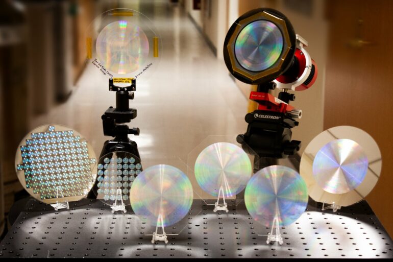
Researchers at the Harvard John A. Paulson School of Engineering and Applied Sciences (SEAS) have developed a 10-centimeter-diameter glass metalens that can image the sun, the moon and distant nebulae with high resolution. It is the first all-glass, large-scale metalens in the visible wavelength that can be mass produced using conventional CMOS fabrication technology.
The research is published in ACS Nano.
“The ability to accurately control the size of tens of billions of nanopillars over an unprecedentedly large flat lens using state-of-the-art semiconductor foundry processes is a nanofabrication feat that opens exciting new opportunities for space science and technology,” said Federico Capasso, the Robert L. Wallace Professor of Applied Physics and Vinton Hayes Senior Research Fellow in Electrical Engineering at SEAS and senior author of the paper.
Most flat metalenses, which use millions of pillar-like nanostructures to focus light, are about the size of a piece of glitter. In 2019, Capasso and his team developed a centimeter-scale metalens using a technique called deep-ultraviolet (DUV) projection lithography, which projects and forms a nanostructure pattern that can be directly etched into the glass wafer, eliminating the time-consuming writing and deposition processes that were required for previous metalenses.
DUV projection lithography is commonly used to pattern fine lines and shapes in silicon chips for smartphones and computers. Joon-Suh Park, a former graduate student at SEAS and current postdoctoral fellow in Capasso’s team demonstrated that the technique could not only be used to mass produce metalenses but also increase their size for applications in virtual and augmented reality.
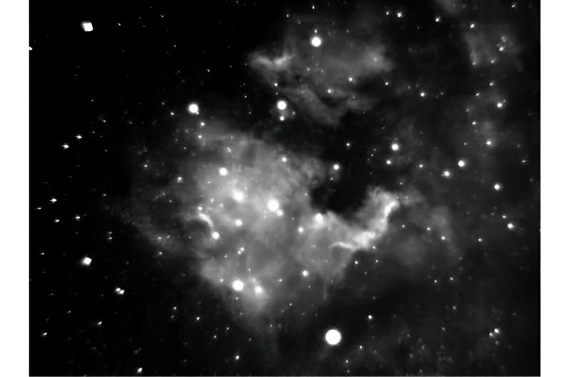
Image of the North America Nebula, in the constellation Cygnus, taken by the metalens on the roof of the Science Center in Cambridge. © Capasso Lab/Harvard SEAS
But making the metalens even larger for applications in astronomy and free-space optical communications posed an engineering problem.
“There is a major limitation with the lithography tool because these tools are used to make computer chips, so chip size is restricted to no more than 20 to 30 millimeters,” said Park, co-first author of the paper. “In order to make a 100-millimeter diameter lens, we needed to find a way around this limitation.”
Park and the team developed a technique to stitch together several patterns of nanopillars using the DUV projection lithography tool. By dividing the lens into 25 sections but using only the seven sections of a quadrant considering the rotational symmetry, the researchers showed that DUV projection lithography could pattern 18.7 billion designed nanostructures onto a 10-centimeter circular area in a matter of minutes.
The team also developed a vertical glass etching technique that allows the creation of high-aspect ratio, smooth-sidewall nanopillars etched into glass.
“Using the same DUV projection lithography, one could produce large-diameter, aberration-correcting meta-optics or even larger lenses on larger glass diameter wafers as the corresponding CMOS foundry tools become increasingly available in the industry,” said Soon Wei Daniel Lim, a postdoctoral fellow at SEAS and co-first author of the paper.
Lim played a lead role in the full simulation and characterization of all the possible fabrication errors that could arise during mass-manufacturing processes and how they could impact the optical performance of metalenses.
After addressing possible manufacturing challenges, the researchers demonstrated the power of the metalens in imaging celestial objects.
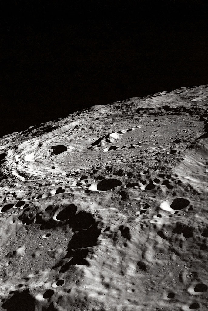
Mounting the metalens on a tripod with a color filter and camera sensor, Park and the team took to the roof of Harvard’s Science Center. There, they imaged the sun, the moon and the North America nebula, a dim nebula in the constellation Cygnus about 2,590 light years away.
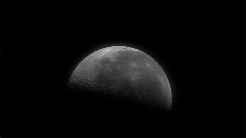
Image of the moon taken by the metalens from the roof a building in Cambridge, MA. © Capasso Lab/Harvard SEAS
“We were able to get very detailed images of the sun, the moon and the nebula that are comparable to images taken by conventional lenses,” said Arman Amirzhan, a graduate student in the Capasso Lab and co-author of the paper.
Using only the metalens, the researchers were able to image the same cluster of sunspots as a NASA image taken that same day.
The team also demonstrated that the lens could survive exposure to extreme heat, extreme cold and the intense vibrations that would occur during a space launch without any damage or loss in optical performance.
Because of its size and monolithic glass composition, the lens could also be used for long-range telecommunications and directed energy transport applications.
More information:
Joon-Suh Park et al, All-Glass 100 mm Diameter Visible Metalens for Imaging the Cosmos, ACS Nano (2024). DOI: 10.1021/acsnano.3c09462
Provided by
Harvard John A. Paulson School of Engineering and Applied Sciences
Citation:
Large, all-glass metalens images sun, moon and nebulae (2024, January 17)
