In most inorganic semiconductors, electrons serve as the primary charge carriers, which limits the development of complementary devices and circuits. A recent study by City University of Hong Kong (CityUHK) researchers has made significant strides in enhancing the mobility of positively charged carriers, known as “holes,” in inorganic semiconductors.
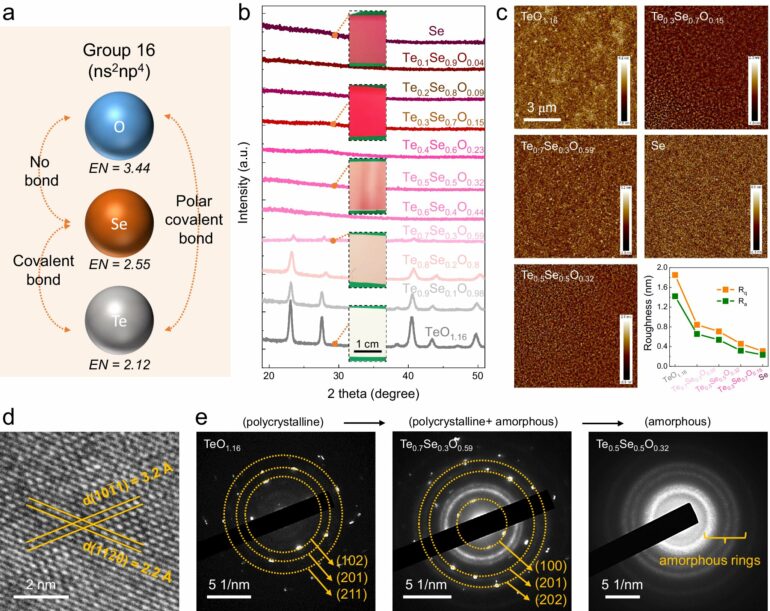
The research team achieved this breakthrough by employing an innovative inorganic blending strategy, combining various intrinsic p-type inorganic materials into a single compound, called tellurium-selenium-oxygen (TeSeO).
The TeSeO materials have shown remarkable adaptability and reliability, and they are a promising solution to address the challenges with current semiconductors.
“This breakthrough opens new possibilities for creating high-performance and cost-effective devices and circuits in the future,” said Professor Johnny Ho, Associate Vice-President (Enterprise) and Professor in the Department of Materials Science and Engineering, who led the study.
Professor Ho further explained, “We have successfully developed air-stable, high-mobility TeSeO thin-film transistors and flexible photodetectors that surpass conventional p-type semiconductors, such as metal oxides, metal halides and organic materials. These new devices exhibit remarkable durability and performance, setting a new benchmark in the field.”
The paper is published in the journal Nature Communications.
One of the major challenges in this research was the difficulty in continuously adjusting the bandgap of conventional p-type semiconductors. However, by rationally combining different types of inorganic materials, the team was able to engineer the band structure of TeSeO and achieve tunable bandgaps ranging from 0.7 to 2.2 eV.
Using the inorganic blending strategy, the research team engineered the band structure of TeSeO to meet specific technical requirements. The tunable bandgaps of TeSeO thin films cover a wide range of wavelengths, including ultraviolet, visible and short-wave infrared regions. This opens exciting possibilities for applications such as high-mobility p-channel transistors, solar cells and wideband photodetectors.
“In the future, we plan to further explore and optimize these applications to harness the full potential of TeSeO materials,” said Professor Ho.

More information:
You Meng et al, An inorganic-blended p-type semiconductor with robust electrical and mechanical properties, Nature Communications (2024). DOI: 10.1038/s41467-024-48628-z
Provided by
City University of Hong Kong
Citation:
Enhancing semiconductor functionality with TeSeO materials for future electronics (2024, September 26)