Silicon transistors, which are used to amplify and switch signals, are a critical component in most electronic devices, from smartphones to automobiles. But silicon semiconductor technology is held back by a fundamental physical limit that prevents transistors from operating below a certain voltage.
This limit, known as “Boltzmann tyranny,” hinders the energy efficiency of computers and other electronics, especially with the rapid development of artificial intelligence technologies that demand faster computation.
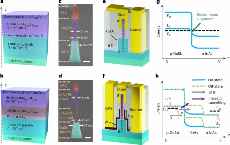
In an effort to overcome this fundamental limit of silicon, MIT researchers fabricated a different type of three-dimensional transistor using a unique set of ultrathin semiconductor materials. The research appears in Nature Electronics.
Their devices, featuring vertical nanowires only a few nanometers wide, can deliver performance comparable to state-of-the-art silicon transistors while operating efficiently at much lower voltages than conventional devices.
“This is a technology with the potential to replace silicon, so you could use it with all the functions that silicon currently has, but with much better energy efficiency,” says Yanjie Shao, an MIT postdoc and lead author of a paper on the new transistors.
The transistors leverage quantum mechanical properties to simultaneously achieve low-voltage operation and high performance within an area of just a few square nanometers. Their extremely small size would enable more of these 3D transistors to be packed onto a computer chip, resulting in fast, powerful electronics that are also more energy-efficient.
“With conventional physics, there is only so far you can go. The work of Yanjie shows that we can do better than that, but we have to use different physics. There are many challenges yet to be overcome for this approach to be commercial in the future, but conceptually, it really is a breakthrough,” says senior author Jesús del Alamo, the Donner Professor of Engineering in the MIT Department of Electrical Engineering and Computer Science (EECS).
They are joined on the paper by Ju Li, the Tokyo Electric Power Company Professor in Nuclear Engineering and professor of materials science and engineering at MIT; EECS graduate student Hao Tang; MIT postdoc Baoming Wang; and professors Marco Pala and David Esseni of the University of Udine in Italy.
Surpassing silicon
In electronic devices, silicon transistors often operate as switches. Applying a voltage to the transistor causes electrons to move over an energy barrier from one side to the other, switching the transistor from “off” to “on.” By switching, transistors represent binary digits to perform computation.
A transistor’s switching slope reflects the sharpness of the “off” to “on” transition. The steeper the slope, the less voltage is needed to turn on the transistor and the greater its energy efficiency.
But because of how electrons move across an energy barrier, Boltzmann tyranny requires a certain minimum voltage to switch the transistor at room temperature.
To overcome the physical limit of silicon, the MIT researchers used a different set of semiconductor materials—gallium antimonide and indium arsenide—and designed their devices to leverage a unique phenomenon in quantum mechanics called quantum tunneling.
Quantum tunneling is the ability of electrons to penetrate barriers. The researchers fabricated tunneling transistors, which leverage this property to encourage electrons to push through the energy barrier rather than going over it.
“Now, you can turn the device on and off very easily,” Shao says.
But while tunneling transistors can enable sharp switching slopes, they typically operate with low current, which hampers the performance of an electronic device. Higher current is necessary to create powerful transistor switches for demanding applications.
Fine-grained fabrication
Using tools at MIT.nano, MIT’s state-of-the-art facility for nanoscale research, the engineers were able to carefully control the 3D geometry of their transistors, creating vertical nanowire heterostructures with a diameter of only 6 nanometers. They believe these are the smallest 3D transistors reported to date.
Such precise engineering enabled them to achieve a sharp switching slope and high current simultaneously. This is possible because of a phenomenon called quantum confinement.
Quantum confinement occurs when an electron is confined to a space that is so small that it can’t move around. When this happens, the effective mass of the electron and the properties of the material change, enabling stronger tunneling of the electron through a barrier.
Because the transistors are so small, the researchers can engineer a very strong quantum confinement effect while also fabricating an extremely thin barrier.
“We have a lot of flexibility to design these material heterostructures so we can achieve a very thin tunneling barrier, which enables us to get very high current,” Shao says.
Precisely fabricating devices that were small enough to accomplish this was a major challenge.
“We are really into single-nanometer dimensions with this work. Very few groups in the world can make good transistors in that range. Yanjie is extraordinarily capable to craft such well-functioning transistors that are so extremely small,” says del Alamo.
When the researchers tested their devices, the sharpness of the switching slope was below the fundamental limit that can be achieved with conventional silicon transistors. Their devices also performed about 20 times better than similar tunneling transistors.
“This is the first time we have been able to achieve such sharp switching steepness with this design,” Shao adds.
The researchers are now striving to enhance their fabrication methods to make transistors more uniform across an entire chip. With such small devices, even a 1-nanometer variance can change the behavior of the electrons and affect device operation.
They are also exploring vertical fin-shaped structures, in addition to vertical nanowire transistors, which could potentially improve the uniformity of devices on a chip.
More information:
Yanjie Shao et al, Scaled vertical-nanowire heterojunction tunnelling transistors with extreme quantum confinement, Nature Electronics (2024). DOI: 10.1038/s41928-024-01279-w
Provided by
Massachusetts Institute of Technology
This story is republished courtesy of MIT News (web.mit.edu/newsoffice/), a popular site that covers news about MIT research, innovation and teaching.
Citation:
Nanoscale transistors could enable more efficient electronics (2024, November 4)


