Dr. Jung-Dae Kwon’s research team at the Energy & Environmental Materials Research Division of the Korea Institute of Materials Science (KIMS) has successfully developed an amorphous silicon optoelectronic device with minimal defects, even using a low-temperature process at 90°C. The findings are published in the journal Advanced Science.
Notably, the team overcame the limitations of high-temperature processing by precisely controlling the hydrogen dilution ratio—the ratio of hydrogen to silane (SiH4) gas—enabling the fabrication of high-performance flexible optoelectronic devices (sensors that detect light and convert it into electrical signals).
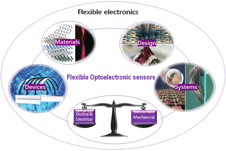
Flexible optoelectronic devices are key components of next-generation electronic devices, such as wearable electronics and image sensors, and require the precise deposition of thin films on thin, bendable substrates. However, a major limitation has been the necessity of high-temperature processing above 250°C, making it difficult to apply these devices to heat-sensitive flexible substrates.
To overcome this limitation, the research team employed precise control of the hydrogen dilution ratio using mass flow controllers during the plasma-enhanced chemical vapor deposition (PECVD) process, which is commonly used for thin-film device fabrication. This approach enabled uniform thin-film quality even at low temperatures.
In addition, by applying hydrogen passivation, they enhanced the electrical performance of the material while minimizing thin-film defects. As a result, they succeeded in fabricating a flexible optoelectronic device that maintained its performance while reducing the processing temperature by more than 60% compared to conventional methods. This substantial reduction in thermal budget also contributes to lowering overall production costs.
")
Photosensitivity Analysis of the Flexible Optoelectronic Device Under a Bent Condition. © Korea Institute of Materials Science (KIMS)
This technology utilizes photoresist (PR) as a sacrificial layer to enable the clean and precise formation of active areas in optoelectronic devices. Photoresist allows stable thin-film deposition even on heat-sensitive flexible substrates and can be easily removed through a simple process, thereby streamlining and improving the efficiency of the entire fabrication process. One of the key advantages of this research outcome is the ability to reliably produce high-quality optoelectronic devices without the need for complex plasma etching processes.
Using this technology, the research team achieved a high photosensitivity—approximately 96% of that of conventional high-temperature processed devices.
Furthermore, after conducting over 2,700 bending tests at a 5 mm bending radius, the device demonstrated excellent mechanical durability and stability with no performance degradation. As a result, this technology is expected to be widely applicable in the fabrication of wearable and flexible electronic devices.
Dr. Jung-Dae Kwon, the principal investigator at KIMS, stated, “This technology demonstrates the potential to fabricate high-quality thin films and high-performance optoelectronic devices without high-temperature processing, simply by precisely controlling the hydrogen dilution ratio.
“We expect this advancement will enable the development of cost-effective and high-performance flexible optoelectronic devices across various applications, including wearable electronics, image sensors, and optical sensors.”
More information:
Ye‐ji Jeong et al, Tailoring Hydrogenation to Enhance Defect Suppression and Charge Transport in Hydrogenated Amorphous Silicon for Flexible Photodetectors, Advanced Science (2025). DOI: 10.1002/advs.202504199
Provided by
National Research Council of Science and Technology
Citation:
Flexible optoelectronic device with minimal defects fabricated at just 90°C (2025, August 1)