A new accelerator chip called Hiddenite that can achieve state-of-the-art accuracy in the calculation of sparse hidden neural networks with lower computational burdens has now been developed by Tokyo Tech researchers. By employing the proposed on-chip model construction, which is the combination of weight generation and supermask expansion, the Hiddenite chip drastically reduces external memory access for enhanced computational efficiency.
Deep neural networks (DNNs) are complex pieces of machine learning architecture for AI that require numerous parameters to learn to predict outputs. DNNs can, however, be “pruned,” thereby reducing the computational burden and model size. A few years ago, the lottery ticket hypothesis took the machine learning world by storm. The hypothesis stated that a randomly initialized DNN contains subnetworks that achieve accuracy equivalent to the original DNN after training. The larger the network, the more “lottery tickets” for successful optimization. These lottery tickets thus allow “pruned” sparse neural networks to achieve accuracy equivalent to more complex, “dense” networks, thereby reducing overall computational burdens and power consumptions.
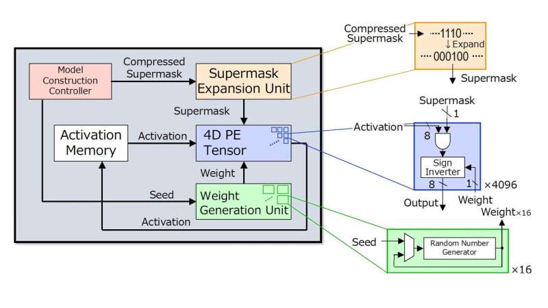
One technique to find such subnetworks is the hidden neural network (HNN) algorithm, which uses AND logic (where the output is only high when all the inputs are high) on the initialized random weights and a “binary mask” called a “supermask” (Fig. 1). The supermask, defined by the top-k% highest scores, denotes the unselected and selected connections as 0 and 1, respectively. The HNN helps reduce computational efficiency from the software side. However, the computation of neural networks also requires improvements in the hardware components.

The new Hiddenite chip offers on-chip weight generation and on-chip “supermask expansion” to reduce external memory access for loading model parameters. © Masato Motomura from Tokyo Tech
Traditional DNN accelerators offer high performance, but they do not consider the power consumption caused by external memory access. Now, researchers from Tokyo Institute of Technology (Tokyo Tech), led by Professors Jaehoon Yu and Masato Motomura, have developed a new accelerator chip called “Hiddenite,” which can calculate hidden neural networks with drastically improved power consumption.
“Reducing the external memory access is the key to reducing power consumption. Currently, achieving high inference accuracy requires large models. But this increases external memory access to load model parameters. Our main motivation behind the development of Hiddenite was to reduce this external memory access,” explains Prof. Motomura. Their study will feature in the upcoming International Solid-State Circuits Conference (ISSCC) 2022, a prestigious international conference showcasing the pinnacles of achievement in integrated circuits.
“Hiddenite” stands for hidden neural network inference tensor engine, and is the first HNN inference chip. The Hiddenite architecture (Fig. 2) offers three-fold benefits to reduce external memory access and achieve high energy efficiency. The first is that it offers the on-chip weight generation for re-generating weights by using a random number generator. This eliminates the need to access the external memory and store the weights. The second benefit is the provision of the “on-chip supermask expansion,” which reduces the number of supermasks that need to be loaded by the accelerator. The third improvement offered by the Hiddenite chip is the high-density four-dimensional (4D) parallel processor that maximizes data re-use during the computational process, thereby improving efficiency.
“The first two factors are what set the Hiddenite chip apart from existing DNN inference accelerators,” says Prof. Motomura. “Moreover, we also introduced a new training method for hidden neural networks, called ‘score distillation,'” in which the conventional knowledge distillation weights are distilled into the scores because hidden neural networks never update the weights. The accuracy using score distillation is comparable to the binary model while being half the size of the binary model.”

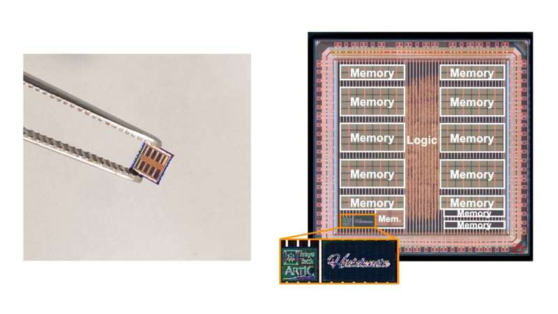
Fabricated using 40nm technology, the core of the chip area is only 4.36 square millimeters. © Masato Motomura from Tokyo Tech
Based on the Hiddenite architecture, the team has designed, fabricated, and measured a prototype chip with Taiwan Semiconductor Manufacturing Company’s (TSMC) 40nm process (Fig. 3). The chip is only 3mm x 3mm and handles 4,096 MAC (multiply-and-accumulate) operations at once. It achieves a state-of-the-art level of computational efficiency, up to 34.8 trillion or tera operations per second (TOPS) per Watt of power, while reducing the amount of model transfer to half that of binarized networks.
These findings and their successful exhibition in a real silicon chip are sure to cause another paradigm shift in the world of machine learning, paving the way for faster, more efficient, and ultimately more environmentally-friendly computing.
More information:
Hiddenite: 4K-PE Hidden Network Inference 4D-Tensor Engine Exploiting On-Chip Model Construction Achieving 34.8-to-16.0TOPS/W for CIFAR-100 and ImageNet, 15.4, ML Processors LIVE Q&A with demonstration, February 23 9:00AM PST, International Solid-State Circuits Conference 2022 (ISSCC 2022). www.isscc.org/
Provided by
Tokyo Institute of Technology
Citation:
Hiddenite: A new AI processor for reduced computational power consumption based on a cutting-edge neural network theory (2022, February 18)


