The transformative changes brought by deep learning and artificial intelligence are accompanied by immense costs. For example, OpenAI’s ChatGPT algorithm costs at least $100,000 every day to operate. This could be reduced with accelerators, or computer hardware designed to efficiently perform the specific operations of deep learning. However, such a device is only viable if it can be integrated with mainstream silicon-based computing hardware on the material level.
This was preventing the implementation of one highly promising deep learning accelerator—arrays of electrochemical random-access memory, or ECRAM—until a research team at the University of Illinois Urbana-Champaign achieved the first material-level integration of ECRAMs onto silicon transistors. The researchers, led by graduate student Jinsong Cui and professor Qing Cao of the Department of Materials Science & Engineering, recently reported an ECRAM device designed and fabricated with materials that can be deposited directly onto silicon during fabrication in Nature Electronics, realizing the first practical ECRAM-based deep learning accelerator.
“Other ECRAM devices have been made with the many difficult-to-obtain properties needed for deep learning accelerators, but ours is the first to achieve all these properties and be integrated with silicon without compatibility issues,” Cao said. “This was the last major barrier to the technology’s widespread use.”
ECRAM is a memory cell, or a device that stores data and uses it for calculations in the same physical location. This non-standard computing architecture eliminates the energy cost of shuttling data between the memory and the processor, allowing data-intensive operations to be performed very efficiently.
ECRAM encodes information by shuffling mobile ions between a gate and a channel. Electrical pulses applied to a gate terminal either inject ions into or draw ions from a channel, and the resulting change in the channel’s electrical conductivity stores information. It is then read by measuring the electric current that flows across the channel. An electrolyte between the gate and the channel prevents unwanted ion flow, allowing ECRAM to retain data as a non-volatile memory.

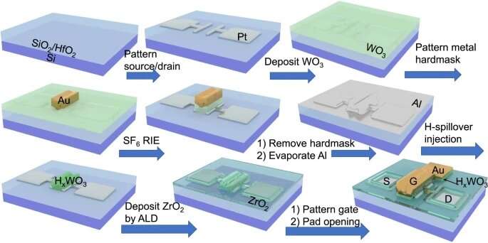
ECRAM fabrication flow. © Nature Electronics (2023). DOI: 10.1038/s41928-023-00939-7
The research team selected materials compatible with silicon microfabrication techniques: tungsten oxide for the gate and channel, zirconium oxide for the electrolyte, and protons as the mobile ions. This allowed the devices to be integrated onto and controlled by standard microelectronics. Other ECRAM devices draw inspiration from neurological processes or even rechargeable battery technology and use organic substances or lithium ions, both of which are incompatible with silicon microfabrication.
In addition, the Cao group device has numerous other features that make it ideal for deep learning accelerators. “While silicon integration is critical, an ideal memory cell must achieve a whole slew of properties,” Cao said. “The materials we selected give rise to many other desirable features.”
Since the same material was used for the gate and channel terminals, injecting ions into and drawing ions from the channel are symmetric operations, simplifying the control scheme and significantly enhancing reliability. The channel reliably held ions for hours at time, which is sufficient for training most deep neural networks. Since the ions were protons, with the smallest ion, the devices switched quite rapidly. The researchers found that their devices lasted for over 100 million read-write cycles and were vastly more efficient than standard memory technology. Finally, since the materials are compatible with microfabrication techniques, the devices could be shrunk to the micro- and nanoscales, allowing for high density and computing power.
The researchers demonstrated their device by fabricating arrays of ECRAMs on silicon microchips to perform matrix-vector multiplication, a mathematical operation crucial to deep learning. Matrix entries (neural network weights) were stored in the ECRAMs, and the array performed the multiplication on the vector inputs, represented as applied voltages, by using the stored weights to change the resulting currents. This operation as well as the weight update was performed with a high level of parallelism.
“Our ECRAM devices will be most useful for AI edge-computing applications sensitive to chip size and energy consumption,” Cao said. “That’s where this type of device has the most significant benefits compared to what is possible with silicon-based accelerators.”
The researchers are patenting the new device, and they are working with semiconductor industry partners to bring this new technology to market. According to Cao, a prime application of this technology is in autonomous vehicles, which must rapidly learn their surrounding environment and make decisions with limited computational resources. Cao is collaborating with Illinois electrical & computer engineering faculty to integrate their ECRAMs with foundry-fabricated silicon chips and Illinois computer science faculty to develop software and algorithms taking advantage of ECRAM’s unique capabilities.
More information:
Jinsong Cui et al, CMOS-compatible electrochemical synaptic transistor arrays for deep learning accelerators, Nature Electronics (2023). DOI: 10.1038/s41928-023-00939-7
Provided by
University of Illinois Grainger College of Engineering
Citation:
Researchers achieve the first silicon integrated ECRAM for a practical AI accelerator (2023, March 28)


