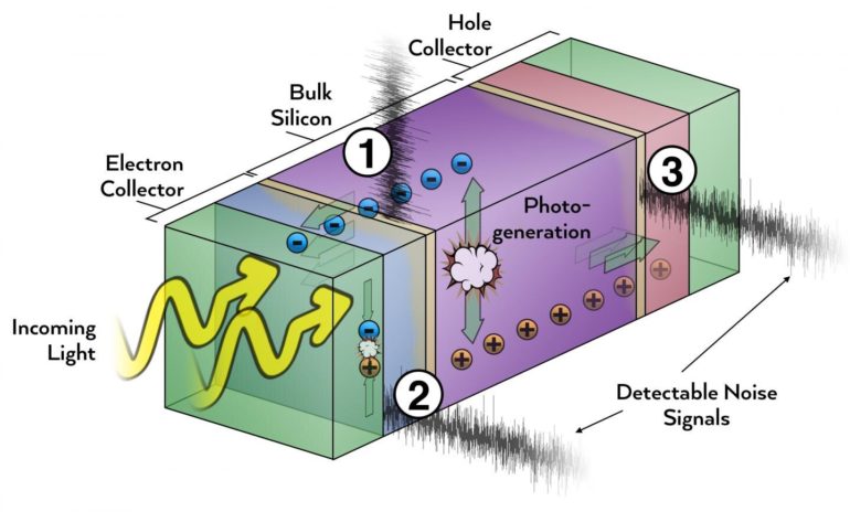
As society moves towards a renewable energy future, it’s crucial that solar panels convert light into electricity as efficiently as possible. Some state-of-the-art solar cells are close to the theoretical maximum of efficiency—and physicists from the University of Utah and Helmholtz-Zentrum Berlin have figured out a way to make them even better.
In a new study, physicists used a technique known as cross-correlation noise spectroscopy to measure miniscule fluctuations in electrical current flowing between materials inside silicon solar cells. The researchers identified crucial electrical noise signals that are completely invisible to conventional noise-measuring methods. They were also able to pinpoint the likely physical processes causing the noise, which often results in a loss of energy and lower efficiency.
“Measuring noise on an object is relatively simple. You can just buy devices that do it. But the problem that plagues us is that these devices also have noise,” said Kevin Davenport, associate instructor of physics at the U and lead author of the paper. “This cross-correlation technique allows us to not only measure the noise of the device, but to also measure the noise of our detector and remove it so that we can see much, much smaller noise signals.”
The technique, that was published on June 24 in the journal Scientific Reports, is an important new tool to improve material interfaces for a better solar cell, or to analyze inefficiencies in other complicated devices.
“It’s surprising how important tiny improvements in efficiency is for industry. Just a fraction of a percent improvement translates into billions of dollars because of the scale of production,” said co-author Klaus Lips, professor of physics at Freie Universität Berlin and department head at Helmholtz-Zentrum Berlin where the solar cells have been designed and fabricated.
“In the past, we have used the cross-correlation technique to study fairly simple research-grade light emitting diodes, but advantages of the method truly came into the light in this work,” said Andrey Rogachev, professor of physics at the U and co-author of the study. “And it goes beyond the solar industry. In any device with many layers, each interface between materials can diminish efficiency in some way. It’s so complicated, you have to be really discreet to be able to say what’s going on and, more importantly, where the particular noise is happening. It turns out that this technique allows us to do just that.”
As often happens in modern research, a single method was not enough to understand complex devices. Interpretation of the noise date have been heavily helped by solar cell simulations carried out by C.T. Trinh, a postdoctoral researcher at Helmholtz-Zentrum Berlin and co-author of the study. The final co-author is Mark Hayward, then an undergraduate research at the U and now a graduate student at University of California, Irvine.
Analyzing noise
The study analyzed silicon heterojunction solar cells (HSCs), a high-end type of single-material solar cell and currently the most efficient of its kind on the market—26.7% of light that hits the cell is converted into electricity. In contrast, the cells that make up solar panels on a residential house range between 15% and 20% efficiency.
In an HSC, electricity generation starts when individual particles of light called photons are absorbed by the photo-active layer made of crystalline silicon and creates pairs of negatively charged electrons and positively charged holes, which are charges caused by missing electrons. Electrons and holes are then pulled in opposite directions by an electrical field created by two selective contacts made of hydrogenated amorphous silicon modified with impurities. This process produces current that we use as electricity. The problem is that the selective electrode and photo-active silicon do not match together perfectly, creating defects that trap electrons. To eliminate these defects in research-grade solar cells like the ones in the study, the scientists place between them an ultrathin layer of pure amorphous silicon. Finally, all of these five layers are sandwiched between two layers of transparent conducting material, known as ITO, and gold electrodes.
The efficiency of HSCs depends on how well the different layers are connected together. A slight mismatch between two layers can make it difficult for the electrons to get where they need to go—a problem that will produce a noise signal.
“That problem is kind of hidden inside these interfaces, and it’s really difficult to be able to detect any kind of signal. But the noise technique that we use is very sensitive to really, really small individual signals,” said Davenport. It’s like listening to a note played by different instruments, he continued. A C-note on a violin is the same as a C-note on a cello, but they sound different. If you were to analyze that note, you can pull out information to learn something about the instrument that produced it, like the length or material of the strings.
“We do something similar to that. We see this wide spectrum of different noise signals and different positions along the frequency axis. We can say, ‘OK, this part of the note that we see, we can attribute to this physical process and this part is a different physical process,'” said Davenport. “But the device is full of these processes that all generate noise and it’s really difficult to un-entangle them—like pulling out a single voice in a 200-person chorus. This technique allows us to remove a lot of the unwanted portion of the signal.”
Mapping inefficiencies
The silicon HSCs are excellent as they are, but they still have limits. The research team’s new technique identified key areas in the device where specific physical processes are producing electrical signals. In the future, small adjustments at these stages could improve the efficiency of these cells, and solar cells of the future. After sifting through the electrical cacophony to discover the relevant signals, the physicists ran a simulation to pinpoint what physical processes were happening at the location of the signal.
The next generation of solar cells are known as tandem cells, which are stacks of different photovoltaic materials that are each sensitive to a different part of the sun’s light, giving such a device an ability to generate more energy. One proposed device layer is the hot-ticket perovskite material.
“Together, the new solar cell can break through the limit of the silicon device by itself, beyond 30% efficiency,” said Lips.
At this edge of efficiency, small losses matter. One such loss has been observed by material scientists; the deposition of the transparent ITO somehow modifies the underlying silicon layers, creating defects which reduce the device’s efficiency. One of the major electrical noise signals that the researchers identified in this study was at this interface, where the charges are trapped and released. Another major signal occurred as holes passed through a similar barrier on the back side of the device.
“The ability to detect these signals means that we can understand their sources and mitigate them,” said Davenport.
Scientists develop transparent electrode that boosts solar cell efficiency
More information:
Kevin Davenport et al, Relaxation processes in silicon heterojunction solar cells probed via noise spectroscopy, Scientific Reports (2021). DOI: 10.1038/s41598-021-92866-w
Provided by
University of Utah
Citation:
Cutting through noise for better solar cells (2021, July 7)
retrieved 8 July 2021
from https://techxplore.com/news/2021-07-noise-solar-cells.html
This document is subject to copyright. Apart from any fair dealing for the purpose of private study or research, no
part may be reproduced without the written permission. The content is provided for information purposes only.


