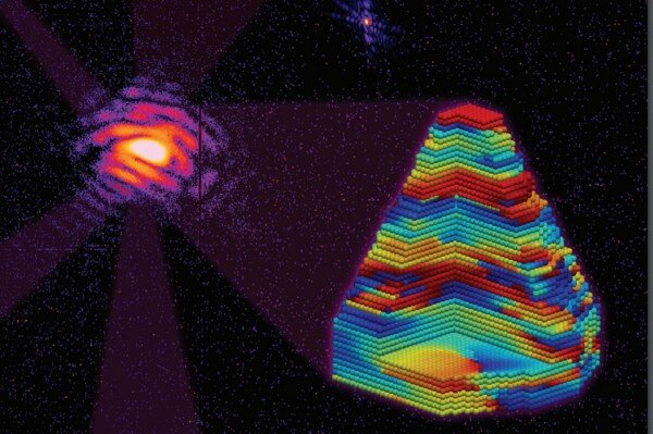
Researchers led by Edwin Fohtung, an associate professor of materials science and engineering at Rensselaer Polytechnic Institute, have developed a new technique for revealing defects in nanostructured vanadium oxide, a widely used transition metal with many potential applications including electrochemical anodes, optical applications, and supercapacitors. In the research—which was published in an article in the Royal Chemical Society journal CrystEngComm, and also featured on the cover of the edition—the team detailed a lensless microscopy technique to capture individual defects embedded in vanadium oxide nanoflakes.
“These observations could help explain the origin of defects in structure, crystallinity, or composition gradients observed near grain boundaries in other thin-film or flake technologies,” said Fohtung, an expert in novel synchrotron scattering and imaging techniques. “We believe that our work has the potential to change how we view the growth and non-destructive three-dimensional imaging of nanomaterials.”
Vanadium oxide is currently used in many technological fields such as energy storage, and can also be used in constructing field-effect transistors owing to metal insulating transition behavior that can be adjusted with an electric field. However, strain and defects in the material can alter its functionality, creating the need for non-destructive techniques to detect those potential flaws.
The team developed a technique based on coherent X-ray diffraction imaging. This technique relies on a type of circular particle accelerator known as a synchrotron. Synchrotrons work by accelerating electrons through sequences of magnets until they reach almost the speed of light. These fast-moving electrons produce very bright intense light, predominantly in the X-ray region. This synchrotron light, as it is named, is millions of times brighter than light produced from conventional sources and 10 billion times brighter than the sun. Fohtung and his students have successfully used this light to develop techniques and capture minute matter such as atoms and molecules and now defects. When used to probe crystalline materials, this technique is known as Bragg coherent diffraction imaging (BCDI). In their research, the team used a BCDI approach to reveal nanoscale properties of electron densities in crystals, including strain and lattice defects.
Fohtung worked closely with Jian Shi, a Rensselaer associate professor of materials science and engineering. They were joined in the research on “Imaging defects in vanadium(III) oxide nanocrystals using Bragg coherent diffractive imaging” by Zachary Barringer, Jie Jiang, Xiaowen Shi, and Elijah Schold at Rensselaer, as well as researchers at Carnegie Mellon University.
Big data technique reveals previously unknown capabilities of common materials
More information:
Zachary Barringer et al, Imaging defects in vanadium(iii) oxide nanocrystals using Bragg coherent diffractive imaging, CrystEngComm (2021). DOI: 10.1039/D1CE00736J
Provided by
Rensselaer Polytechnic Institute
Citation:
Imaging technique reveals strains and defects in vanadium oxide (2021, October 14)
retrieved 15 October 2021
from https://phys.org/news/2021-10-imaging-technique-reveals-strains-defects.html
This document is subject to copyright. Apart from any fair dealing for the purpose of private study or research, no
part may be reproduced without the written permission. The content is provided for information purposes only.


