November 19, 2020
feature
To fabricate nanoscale photonic and electronic devices, engineers need electrodes made of asymmetric metals separated by gaps in the nanometer (nm) length scale. So far, most of these electrodes were fabricated using high-end patterning techniques, such as electron-beam lithography.
While electron-beam lithography has been found to enable high-fidelity patterning in asymmetric metal electrodes, it also comes with a number of limitations. For instance, it is typically very difficult to apply on a larger scale, as it can only process a limited number of items simultaneously and it is only effective on some materials.
Researchers at King Abdullah University of Science and Technology (KAUST) and Imperial College London introduced an alternative method that could be potentially used to fabricate asymmetric nanogap electrodes on a large scale. Recently, they used this technique, first presented a few years ago in a paper published in Nature Communications, to fabricate nanogap electrode devices.
“Our recent study is based on a serendipitous discovery that my group made back in 2014; that of a method (i.e., adhesion-lithography or ‘a-Lith’) that can be used to pattern two electrodes made of the same or different metals less than 15 nm apart from each other,” Thomas D. Anthopoulos, the lead researcher who carried out the study, told TechXplore. “Although our initial interest was to fabricate self-aligned gate transistors, we soon realized that the self-aligned electrodes were separated by a tiny distance (i.e., a nanogap that is
The fabrication method devised by Anthopoulos and his colleagues does not require particularly sophisticated tools and can also be applied over large parts of materials using traditional lithographic equipment. Moreover, it can achieve good results without having to employ additional and typically expensive patterning techniques such as electron beam lithography.
When they first started testing their method approximately a half-decade ago, the researchers primarily used it to create organic optoelectronic nanogap devices. However, they soon realized that it also allowed for inorganic materials, such as ZnO, to be deposited inside the nanogap using a precursor solution.
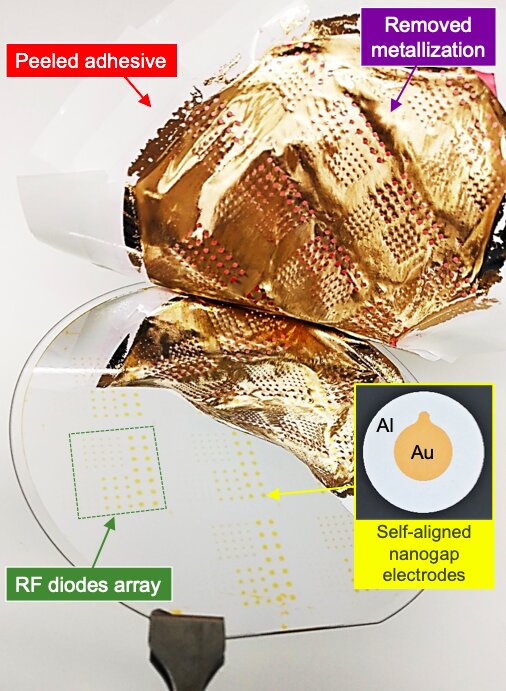
In their recent study, Anthopoulos and his colleagues used their a-Lith technique to create solution-processed ZnO Schottky diodes that can operate at microwave and millimeter-wave frequency bands. To create these diodes, they used wafer-scale a-Lith to pattern two asymmetric metal electrodes, separating them with a gap of approximately 15 nm. Finally, they completed them by depositing a ZnO layer on the device substrate.
“The fact that a-Lith allows for two different metals to be aligned so close to each other, allowed us to tune the properties of two metal-ZnO contacts individually making one Ohmic and the other -15 nm away- rectifying so the overall planar device behaves like a diode (i.e., a device allowing flow of current only in one direction),” Anthopoulos said. “The nanoscale dimension of this critical device parameter is the reason for the exceptional operating characteristics of our planar ZnO Schottky diodes.”
The a-Lith fabrication process is fairly simple and could thus be easier to implement on a large scale. It also does not require a precise control of the deposition parameters, which is usually necessary when creating conventional vertical-type diodes.
“Our diodes can be easily fabricated over large area substrates (glass, silicon or even polymers) using conventional lithography in combination with a few key processing steps,” Anthopoulos said. “These steps enable the formation of the nanogap between two overlapping metal electrodes, upon mechanical peeling of an adhesive layer that we apply atop the two metal electrodes. Once the asymmetric nanogap electrodes were formed, a precursor solution of the ZnO or the Al-doped ZnO was deposited atop via spin coating, followed by a final thermal annealing step in air.”
The diodes fabricated by Anthopoulos exhibit a maximum intrinsic cut-off frequency of 100 GHz. Moreover, the researchers integrated them with other passive electronic components to create radio-frequency energy-harvesting circuits and found that these circuits achieved output voltages of 600 mV and 260 mV at 2.45 GHz and 10 GHz, respectively.
“The a-Lith method serves as a powerful example of how up-scalable bottom-up techniques can be cleverly combined with established top-down methods to produce innovative processing paradigms that offer unique advantages over traditional manufacturing technologies,” Anthopoulos said. “Our ZnO diodes demonstrate, for the first time, how our processing paradigm can yield devices that are able to operate at frequencies previously unimaginable for solution-processed, large-area electronics, especially for the internet of things (IoT) device ecosystem.”
The same design and fabrication process used to create these Schottky diodes could also theoretically be applied to the development of other circuit components, including resistors and capacitors. In the future, this study could pave the way toward the development and large-scale manufacturing of numerous devices, as well as monolithic radio frequency (RF) circuits without the need for expensive and often unreliable heterogeneous component integration processes.
“I feel that our work bridges the worlds of traditional RF electronics with the emerging field of printed large-area electronics and has the potential to enable a host of new applications,” Anthopoulos said. “We are now working on a number of projects utilizing our nanogap technology, including the development of improved and highly scalable nanolithography techniques that offer improved resolution while being simpler to implement and that of innovative optoelectronics, sensors and energy harvesting/generating devices. The future is definitely bright for our large-size yet tiny nanogaps.”
High-resolution lithography for nanoporous thin films
More information:
Dimitra G. Georgiadou et al. 100 GHz zinc oxide Schottky diodes processed from solution on a wafer scale, Nature Electronics (2020). DOI: 10.1038/s41928-020-00484-7
David J. Beesley et al. Sub-15-nm patterning of asymmetric metal electrodes and devices by adhesion lithography, Nature Communications (2014). DOI: 10.1038/ncomms4933
2020 Science X Network
Citation:
Nanoscale Schottky diodes fabricated via adhesion lithography (2020, November 19)
retrieved 20 November 2020
from https://techxplore.com/news/2020-11-nanoscale-schottky-diodes-fabricated-adhesion.html
This document is subject to copyright. Apart from any fair dealing for the purpose of private study or research, no
part may be reproduced without the written permission. The content is provided for information purposes only.


