Physicists have found a way to make transistors using materials that are highly rated for their performance in next-generation solar cells and light-emitting diodes (LEDs). The researchers have overcome the problem of the material’s ion content interfering with the flow of electronic current through a transistor. This breakthrough may pave the way for research into greener electronic components for low-cost electronic devices.
Over the past decade, solution-processed metal-halide perovskites (a hybrid metal-organic material) have been a major focus of research into low-cost, high-efficiency solar cells and LEDs. Because of their ability to process at relatively low temperatures, perovskites are considered a greener alternative to silicon, not only for the fabrication of solar cells but also for transistors. A transistors is the building blocks of an integrated circuit, and the key component in many electronic devices.
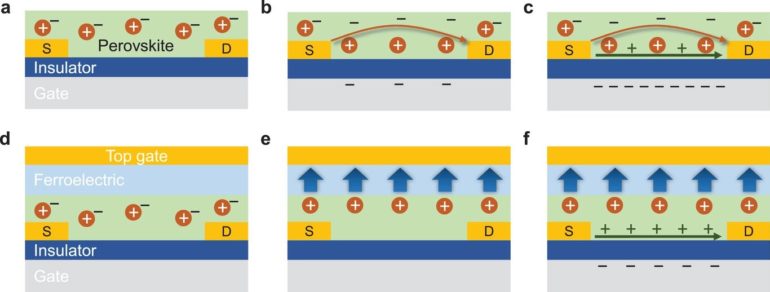
Transistors operate through a gate system: electrons flow between a “source” and a “drain,” and their flow is controlled by an electric field applied to the “gate.” In a transistor, the presence of ions interferes with the flow of electronic current, rendering the transistor inoperable. Metal-halide perovskites are rich in ions. When an electric field is applied to a perovskite, these ions respond to the electric field by rushing to the gate and accumulating there, effectively blocking the flow of electrons between the source and the drain.
To counter this interference, scientists have spent the past decade searching for ways to stymie the ions, manipulating them to minimize their adverse impacts on the perovskite transistor.
Scientists from the University of Bath and the Max Planck Institute for Polymer Research (MPIP) in Germany have found a solution to the perovskite problem, enabling the material to work as a transistor at room temperature. The device has been “tricked” into ignoring the material’s ion content by shunting these electrically charged species away from the gate to a different part of the transistor, where they can’t interfere with the flow of current.
“Until now, the presence of ions in perovskites has rendered the use of perovskites in transistors challenging. We saw this as a shame since perovskites are very promising semiconducting materials,” said lead researcher Professor Kamal Asadi from the Department of Physics at the University of Bath.
He added: “At room temperature, the perovskite’s ions are pretty mobile. People have resorted to reducing the temperature to get perovskite transistors to work because at low temperatures, ions are less mobile. But in real-life applications, that would mean that our perovskite-based gadgets would only operate reliably in the fridge or in Antarctica.”
“We looked at the problem from a different angle. We modified the construction of the transistors instead of modifying the material, resulting in a transistor with an extra, auxiliary gate. Ions are then pushed to the auxiliary gate and fixed in position. Then, when you apply a gate electric field, the electrons now see the gate field, react to it, and an electron flow between the source and the drain is established.”
The auxiliary gate was created by depositing a ferroelectric layer onto the transistor. Ferroelectrics (dielectric materials that show stable polarization when the external electric field is turned off) can induce a large surface charge that attracts ions and holds them in position, thereby freeing up the gate for the flow of electrons. The Bath team is the first to use the concept of ferroelectricity to mitigate ion transport.
“Pushing the ions away from the transport channel can only be achieved with auxiliary gate materials that can induce large surface charges, such as ferroelectrics or electrolytes,” explained the first author of the paper, Dr. Beomjin Jeong, from the Max Planck Institute for Polymer Research. “We chose ferroelectric polymers because of their compatibility and ease of processing on top of the perovskite layer.”
The scientists involved in this project anticipate widespread interest in the platform they have developed, with other researchers widening the hunt for materials with high surface-charge density that can be paired with perovskite. A good degree of control over the number of ions in the transistor channel obtained by a ferroelectric layer is likely to be beneficial for other applications where simultaneous control of ions and electrons is needed.
“Room-temperature halide perovskite field-effect transistors by ion transport mitigation” is published in Advanced Materials.
Germanium-lead perovskite LEDs: A new way to reduce toxicity
More information:
Beomjin Jeong et al, Room‐Temperature Halide Perovskite Field‐Effect Transistors by Ion Transport Mitigation, Advanced Materials (2021). DOI: 10.1002/adma.202100486
Provided by
University of Bath
Citation:
Perovskite allows a greener fabrication of transistors (2021, August 19)
retrieved 20 August 2021
from https://techxplore.com/news/2021-08-perovskite-greener-fabrication-transistors.html
This document is subject to copyright. Apart from any fair dealing for the purpose of private study or research, no
part may be reproduced without the written permission. The content is provided for information purposes only.


