The ability to transmit and manipulate, with minimal loss, the smallest unit of light—the photon—plays a pivotal role in optical communications as well as designs for quantum computers that would use light rather than electric charges to store and carry information.
Now, researchers at the National Institute of Standards and Technology (NIST) and their colleagues have connected, on a single microchip, quantum dots—artificial atoms that generate individual photons rapidly and on-demand when illuminated by a laser—with miniature circuits that can guide the light without significant loss of intensity.
To create the ultra-low-loss circuits, the researchers fabricated silicon-nitride waveguides—the channels through which the photons traveled—and buried them in silicon dioxide. The channels were wide but shallow, a geometry that reduced the likelihood that photons would scatter out of the waveguides. Encapsulating the waveguides in silicon dioxide also helped to reduce scattering.
The scientists reported that their prototype circuits have a loss of intensity equal to only one percent of similar circuits—also using quantum dots—that were fabricated by other teams.
Ultimately, devices that incorporate this new chip technology could take advantage of the strange properties of quantum mechanics to perform complex computations that classical (non-quantum) circuits may not be capable of doing.

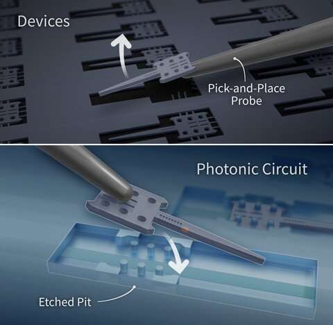
Illustration shows some of the steps in creating the new ultra-low-loss photonic circuit on a chip. A microprobe lifts a gallium arsenide device containing a quantum dot—artificial atoms that generate single photons—from one chip. Then the probe places the quantum-dot device atop a low-loss silver-nitride waveguide built on another chip. © S. Kelley/NIST
For instance, according to the laws of quantum mechanics, a single photon has a probability of residing in two different places, such as two different waveguides, at the same time. Those probabilities can be used to store information; an individual photon can act as a quantum bit, or qubit, which carries much more information than the binary bit of a classical computer, which is limited to a value of 0 or 1.
To perform operations necessary to solve computational problems, these photon qubits—all of which travel at the same speed and are indistinguishable from each other—must simultaneously arrive at specific processing nodes in the circuit. That poses a challenge because photons originating from different locations—and traveling along different waveguides—across the circuit may lie at significantly different distances from processing points. To ensure simultaneous arrival, photons emitted closer to the designated destination must delay their journey, giving those that lie in more distant waveguides a head start.
The circuit devised by NIST researchers including Ashish Chanana and Marcelo Davanco, along with an international team of colleagues, allows for significant time delays because it employs waveguides of various lengths that can store photons for relatively long periods of time. For instance, the researchers calculate that a 3-meter-long waveguide (tightly coiled so its diameter on a chip is only a few millimeters) would have a 50 percent probability of transmitting a photon with a time delay of 20 nanoseconds (billionths of a second). By comparison, previous devices, developed by other teams and operating under similar conditions, were limited to inducing time delays only one one-hundredth as long.
The longer delay times achieved with the new circuit are also important for operations in which photons from one or more quantum dots need to arrive at a specific location at equally spaced time intervals. In addition, the low-loss quantum-dot circuit could dramatically increase the number of single photons available for carrying quantum information on a chip, enabling larger, speedier, and more reliable computational and information-processing systems
The scientists, who include researchers from the University of California, Santa Barbara (UCSB), the Massachusetts Institute of Technology (MIT), the Korea Institute of Science and Technology and the University of São Paulo in Brazil, reported their findings December 11 in Nature Communications.

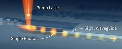
Laser light shining on the quantum dots triggers them to produce a series of single photons that travel through the silicon nitride waveguide. © S. Kelley/NIST
The hybrid circuit consists of two components, each initially built on a separate chip. One, a gallium arsenide semiconductor device designed and fabricated at NIST, hosts the quantum dots and directly funnels the single photons they generate into a second device—a low-loss silicon nitride waveguide developed at UCSB.
To marry the two components, researchers at MIT first used the fine metal tip of a pick-and-place microprobe, acting like a miniature crowbar, to pry the gallium arsenide device from the chip built at NIST. They then placed it atop the silicon nitride circuit on the other chip.
The researchers face several challenges before the hybrid circuit can be routinely employed in a photonic device. At present, only about 6 percent of the individual photons generated by the quantum dots can be funneled into the circuit. However, simulations suggest that if the team changes the angle at which the photons are funneled, in tandem with improvements in the positioning and orientation of the quantum dots, the rate could rise above 80 percent.
Another issue is that the quantum dots do not always emit single photons at exactly the same wavelength, a requirement for creating the indistinguishable photons necessary for the quantum computational operations. The team is exploring several strategies, including applying a constant electric field to the dots, that may alleviate that problem.
More information:
Ashish Chanana et al, Ultra-low loss quantum photonic circuits integrated with single quantum emitters, Nature Communications (2022). DOI: 10.1038/s41467-022-35332-z
Provided by
National Institute of Standards and Technology
This story is republished courtesy of NIST. Read the original story here.
Citation:
Chip circuit for light could be applied to quantum computations (2023, January 3)


