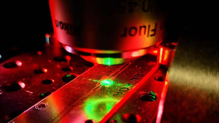
Researchers at TMOS, the ARC Center of Excellence for Transformative Meta-Optical Systems, and their collaborators at RMIT University have developed a new 2D quantum sensing chip using hexagonal boron nitride (hBN) that can simultaneously detect temperature anomalies and magnetic field in any direction in a new, groundbreaking thin-film format.
In their paper published in Nature Communications, they detail a sensor that is significantly thinner than current quantum technology for magnetometry, paving the way for cheaper, more versatile quantum sensors.
To date, quantum sensing chips have been made from diamond as it’s a very robust platform. The limitations of diamond-based sensors, though, is that they can only detect magnetic fields when aligned in the direction of the field. If unaligned, they have large blind spots. As a result, magnetometers made of diamond must contain multiple sensors at varying degrees of alignment.
This increases the difficulty of operation and, as a result, the versatility to use in different applications. In addition, the rigid and three-dimensional nature of the quantum sensor means that its ability to get close to samples that aren’t perfectly smooth is restricted.
TMOS Associate Investigator Jean-Philippe Tetienne (RMIT University) and Chief Investigator Igor Aharonovich (University of Technology Sydney) and their teams are pioneering a new quantum sensing platform using hBN. These hBN crystals are made up of layers of atomically thick sheets and are flexible, which allows the sensing chips to conform to the shape of the sample being studied, getting far closer to the sample than diamond can.
Different defects exist in the hBN that produce different optical phenomena. A recently discovered carbon-based defect, the atomic structure of which remains unidentified, detects magnetic fields in any direction but until now has not been used for magnetic imaging.
In an effort to determine the structure of the unidentified defect, the team ran a Rabi measurement experiment and compared the results with the well-understood boron vacancy defect that also exists in hBN. This boron vacancy defect can be used to measure temperature at a quantum level. Through this comparison, they discovered the new defect behaves as a spin half system. This half spin nature of the carbon defect is what allows for the sensor to detect magnetic fields in any direction.
The team determined that this new carbon-based half spin sensor could be controlled through electrical excitation, in the same way that the boron vacancy sensor can, and that they could be tuned to interact with one another. Energized by these discoveries, they set out to demonstrate a hBN sensing chip that could use both spin defects simultaneously to measure magnetic field and temperature. Their paper shows the first magnetic images ever taken with this unidentified isotropic sensor.
Co-first author, Sam Scholten from RMIT University says, “Optically addressable spin defects in solids form a vital toolkit in the realm of quantum materials due to their potential to be utilized as nanoscale quantum sensors and more generally as robust room temperate quantum systems.
“What makes hBN unique and exciting is its 2D form, which allows our sensors to get much closer to the sample.”
Co-first author, Priya Singh from RMIT University says, “Diamond spins have been used for over a decade in biological systems as an in-situ probe. I am eager to take our hBN into the continuously moving cellular environment, where the directional independence of the sensor would be an advantage.”
TMOS Chief Investigator Igor Aharonovich says, “hbN has many advantages over diamond as a quantum light source for communications and sensing. In addition to its ultra-thin form factor, it can also operate as a quantum light source for communications at room temperature, where diamond often requires cryogenic cooling. hBN is also much cheaper and more accessible than diamond.”
Generally, these new low-dimensional materials offer the chance of discovering new physics due to their extreme anisotropy. Potential future applications for this quantum sensing technology include in-field identification of magnetic geological features. The spin half nature of the defect will also allow for radio spectroscopy across a wider band than competing technologies.
TMOS Associate Investigator Jean-Phillipe Tetienne says, “The next step for this research is to identify what the atomic defects in the hBN are. By understanding the composition of these, we can make progress toward engineering sensor devices for optimal performance.
“I am excited about exploring the properties and opportunities of this new optical spin defect. Its spin half nature is novel in our community, and there are many questions to answer.”
More information:
Sam C. Scholten et al, Multi-species optically addressable spin defects in a van der Waals material, Nature Communications (2024). DOI: 10.1038/s41467-024-51129-8
Provided by
Australian Research Council
Citation:
New 2D quantum sensor detects temperature anomalies and magnetic fields (2024, August 8)


