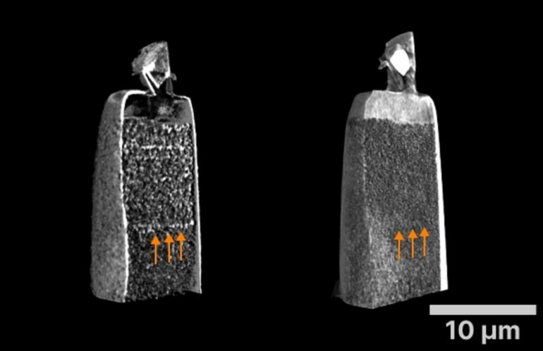
X-ray microscopes are essential for examining components and materials because they can be used to detect changes and details in the material. Until now, however, it has been difficult to detect small cracks or tiny inclusions in the images.
A new method, developed by researchers at the Helmholtz-Zentrum Hereon, allows them to visualize such changes in the nanometer regime. In particular, materials research and quality assurance will profit from this development.
Quality is important in materials science. When metal parts are welded together, you need to know whether the weld seam is any good—or whether small cracks or pores have formed inside, which could lead to failure. High-performance materials, e.g., for electrodes in electric car batteries or fuel cells, should not contain defects and should allow the current to flow undisturbed.
In order to better understand the effects of changes in materials and to detect possible defects, X-rays have already been used for a long time to visualize defects in materials. In conventional X-ray images, structures are made visible through the attenuation of X-rays. However, this is often not sufficient to detect very small or low-density structures.
Combining imaging with scattering
Hereon researchers Sami Wirtensohn and Dr. Silja Flenner from Dr. Imke Greving’s group have now succeeded in making such small structures visible in the nanometer range, using a new method. Unlike a conventional X-ray image, they do not use the attenuated light itself, but rather the light scattered by the object being X-rayed, which is deflected in different directions.
“Nanometer-sized structures such as tiny cracks scatter the light—and this scattering can be seen,” explains Wirtensohn, first author of the study published in Optica. This makes details and structures visible that are normally difficult or impossible to see.
“The method can even make structures visible that are below the resolution of the X-ray microscope,” explains Flenner, who initiated the project.
The challenge with the new approach was that the researchers had to suppress the attenuated light of the object to a certain extent so that the scattering image would become visible. In X-ray microscopy, they therefore use optics that redirect the X-ray light so that the rays follow a known pattern.
These X-ray beams can then be blocked by installing apertures. The scattered light, on the other hand, changes its direction when penetrating the sample and can pass by the apertures. This results in the so-called dark field image, for the first time with nanometer resolution.
“This gives us an image in which the nanostructures are very clearly visible due to the scattering,” says Wirtensohn.
Little effort, big impact
For materials research, this is a gain with little effort. “For the first time, a practical method for dark-field imaging is available that can be easily implemented in an X-ray microscope,” says Greving, who is leading the X-ray microscopy team at the Hereon imaging beamline P05 at the Deutsches Elektronen Synchrotron (DESY).
Such X-ray microscopes are operated at large synchrotron facilities, so-called particle accelerators, of which there are only a few dozen worldwide. These could easily be retrofitted with an aperture to enable dark-field microscopy.
This would be worthwhile because companies or materials researchers would be able to search for tiny defects and flaws in materials much better in future.
More information:
Sami Wirtensohn et al, Nanoscale dark-field imaging in full-field transmission X-ray microscopy, Optica (2024). DOI: 10.1364/OPTICA.524812
Provided by
Helmholtz Association of German Research Centres
Citation:
New method enhances X-ray microscopy for detecting tiny defects (2024, June 18)


