Semiconductors in modern electronics rely on small quantities of added impurity elements, called dopants, that alter the ability of the material to conduct electricity. While the role of these dopants is often straightforward, that isn’t always the case. Electrons from dopants in complex oxides can behave in ways that are significantly different than those in conventional semiconductors, such as silicon.
Researchers who study what happens in these materials typically rely on photoelectron spectroscopy, which measures electrons knocked out of atoms by high-energy light waves. However, this technique requires the atom of interest to be present at or above one percent of the material for a detectable signal. The dopants in many semiconductors are well below those levels, making it challenging to acquire data on them.
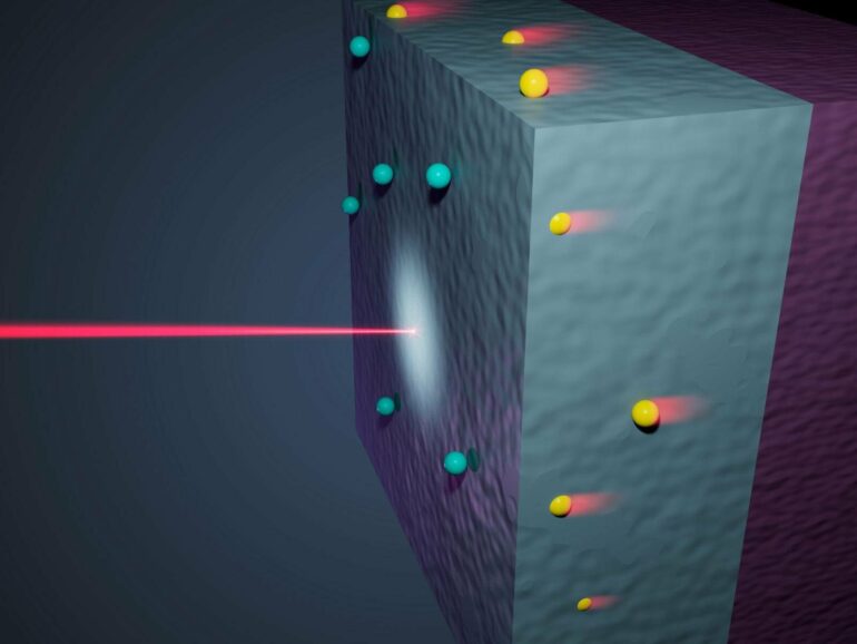
A new study published in Physical Review Materials uses X-ray based resonant photoemission spectroscopy to look at electrons in lightly doped strontium titanium oxide on silicon (STO/Si). Researchers were able to probe and identify the different locations and energies of electrons from the primary dopant in STO/Si. The dopant level was in the thousandths of a percent—substantially lower than can be studied using conventional photoelectron spectroscopy.
In the STO/Si system, “free” and mobile electrons can be one of three primary types. This includes those within the STO film from the primary STO dopant, those from the STO dopant that get trapped at the surface of the STO film, and those that jump from the silicon dopant into the STO. In this new work, the researchers were able to see differences between the dopant electron states in the STO.
Understanding the nuances of electrons
In the studied STO layers, the dopant is not a new atom added to the material but is an atom (oxygen) missing from the material. These oxygen vacancies leave behind two electrons that can conduct electricity. However, these two electrons can also strongly interact with each other, creating a more complicated electronic structure.
Through resonant X-ray photoemission spectroscopy, the team could separately probe the different states that contain the electrons from oxygen vacancies. The experiment was designed to only examine the top layers of the material, avoiding the deeper areas where the dopant electrons from the silicon reside. This creates a much-needed simplification and allows researchers to focus specifically on electrons from the oxygen vacancies.
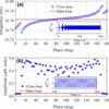
The researchers found that the electrons trapped at the surface have a subtly different energy than the electrons that move freely within the body of the STO. Knowing the energy landscape helps researchers understand how electron trapping at the surface affects the overall electrical conductivity of the STO.
“This approach is incredibly powerful,” said lead author Scott Chambers, a Laboratory Fellow at Pacific Northwest National Laboratory. “We were able to ‘see’ the surface trapped electrons in STO/Si for the first time. I hope others will use this approach to investigate different lightly doped semiconductors with complex electronic structures.”
The work was performed in collaboration with researchers at the University of Texas-Arlington and the Diamond Light Source.
More information:
S. A. Chambers et al, Probing the electronic properties of gap states near the surface of n−SrTiO3−δ/i−Si(001) heterojunctions with high sensitivity, Physical Review Materials (2024). DOI: 10.1103/PhysRevMaterials.8.014602
Provided by
Pacific Northwest National Laboratory
Citation:
New research demonstrates how to study low concentrations of electrons in complex oxide films (2024, February 9)


