Today, lasers are well-established in daily life, even if it is sometimes hard to tell what and where they are. As an example, we can find them in CD/DVD readers or medical applications like cancer and eye surgery, being essential tools in a vast range of multidisciplinary fields. All of this is the result of constant progress and development, from the first Maiman’s ruby laser (1960) to the attosecond lasers, passing through exotic, funny demonstrations like Jell-O lasers.
In the quest to constantly obtain more intense sources, ultrashort lasers (with pulses in the femtosecond regime) represented a clear breakthrough, as they allowed high-intensity delivery in confined spaces on the nanoscale. In particular, they allow inducing nonlinear absorption phenomena which, for instance, permits locally modifying the interior of transparent materials with a low thermal budget, not achievable with other laser sources. Some demonstrations include waveguides writing in glasses or creating 3D complex patterns with polymers.
Ultrafast lasers opened the door to weld stacked transparent materials by irradiating through the top one and focusing on the interface between them. The high intensity results in almost instant local melting and subsequent resolidification, mixing and bonding of both materials. This was demonstrated with several materials including glasses, polymers, ceramics, and metals in diverse configurations.
While ultrafast laser welding would surely find immediate applications in microelectronics, it is striking to realize that the process is not directly applicable to bonding different semiconductor workpieces. The high intensities required for internal glass modification result in strong propagation nonlinearities in semiconductors due to their small bandgap, which tends to defocus and delocalize intense infrared radiation.
In order to tackle this challenge, we had to think outside the box, and what at first seemed to be a step backward resulted in a successful alternative. In the stealth dicing of silicon wafers, infrared nanosecond pulses are used to create defects inside silicon that later serve as weak points to produce clean-edge cuts. The relatively long pulses have lower intensities than ultrashort ones, avoiding undesired propagation nonlinearities, but at the same time, can be absorbed at the focal point by two-photon absorption. Based on this, we moved to longer pulses using these internal modifications not as defects but as strong bonding points.
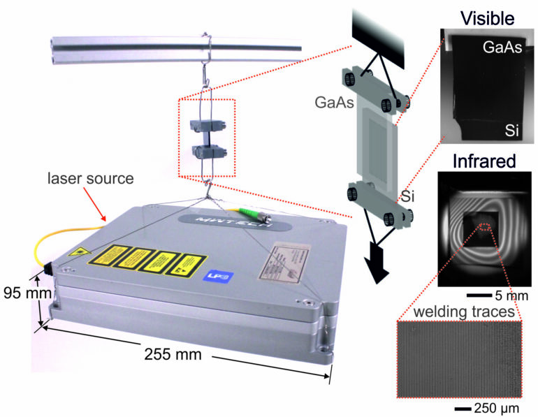
During our first trials of welding silicon pieces, by employing infrared imaging of the interface, we found an added constraint. Unless the gap at the interface is almost nonexistent, including optical contact conditions, the high refractive index typical of semiconductors results in a Fabry-Perot cavity that impedes reaching a high enough energy density to melt both materials. Thus, the most intimate contact between the top and bottom materials is necessary to achieve successful welding.
After setting up the right conditions to circumvent these effects, we successfully made the first experimental demonstration of silicon-silicon laser welding. After an optimization process, we could later extend this approach to other semiconductors such as gallium arsenide in different configurations alongside silicon. Not only did we achieve bonding between different workpieces, but we did so while reaching strong shear force strengths in the order of several tens of MPa. These values compare well to ultrashort laser welding demonstrations of other materials and the currently employed techniques of wafer bonding.
This successful experiment, now published in Laser & Photonics Reviews, confirms a technological barrier that has been definitively lifted. Compared to alternative methods in the semiconductor industry, a unique advantage of laser micro-welding is the ability to join elements with complex multi-material architectures in a direct-write manner that would not be possible otherwise. This should lead to new modalities for manufacturing in electronics, mid-infrared photonics, and microelectromechanical systems (MEMS). Moreover, we envision the potential for the emerging concepts of hybrid chips, including electronics and microfluidics functions for the thermal management of the most demanding micro-technologies, such as super-computers or advanced sensors.
This story is part of Science X Dialog, where researchers can report findings from their published research articles. Visit this page for information about ScienceX Dialog and how to participate.
More information:
Pol Sopeña et al, Transmission Laser Welding of Similar and Dissimilar Semiconductor Materials, Laser & Photonics Reviews (2022). DOI: 10.1002/lpor.202200208
Dr. Pol Sopeña and Dr. David Grojo are researchers at the LP3 laboratory located in Marseille, France. LP3 is a joint unit between the French National Center for Scientific Research (CNRS), and Aix-Marseille University. After earning a Ph.D. at University of Barcelona, Pol Sopeña joined LP3 as a postdoctoral fellow where he now concentrates his work on new semiconductor processing solutions. David Grojo is a permanent CNRS scientist investigating new and exciting opportunities to tailor material properties with non-conventional radiations. His activities are funded by an ERC Consolidator Grant from the Excellence Science pillar of the European Research Council (cordis.europa.eu/project/id/724480).
Citation:
Using lasers to bond semiconductor electronics components (2022, December 5)