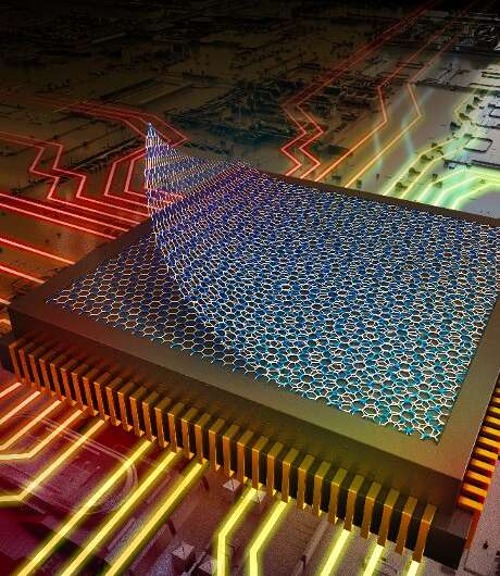
Silicon-based transistors are rapidly approaching their limits, both in terms of speed and performance. Engineers and material scientists have thus been trying to identify alternative materials that could enable the development of faster and better performing devices.
Carbon-based materials are among the most favorable candidates for the development of the next generation of electronics, due to their many advantageous properties, including a high mechanical strength and a good electrical and thermal conductivity. One of the most promising among these materials is graphene, which also exhibits a high flexibility and transparency.
Despite its advantages, graphene has no bandgap, which is an essential requirement for channel materials inside transistors. In recent years, some engineers have thus been conducting studies evaluating an alternative two-dimensional (2D) material that resembles graphene, known as C3N. C3N consists of a uniform distribution of carbon and nitrogen atoms, arranged in a graphene-like structure.
Researchers at University of Queensland in Australia, East China Normal University, Shanghai Institute of Microsystem and Information Technology and other institutes in China have recently demonstrated that the bandgaps of bilayers of 2D C3N can be engineered by changing their stacking order or applying an electric field to them. Their paper, published in Nature Electronics, could pave the way towards the development of better performing C3N-based devices.
“C3N has attractive properties similar to graphene, but in addition, has a medium sized bandgap,” Zhenhui Kang, Debra J. Searles and Qinghong Yuan, three of the researchers who carried out the study, told Tech Xplore via email. “We therefore thought that we might be able to tune the properties of the C3N monolayer by forming different bilayers and changing its environment by applying an electric field.”
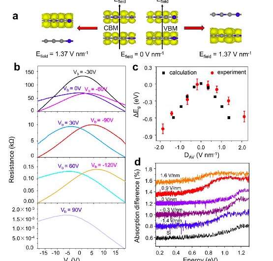
Kang, Searles, Yuan and their colleagues carried out a series of theoretical calculations and experiments aimed at investigating the potential of C3N as a material to develop the next generation of electronic devices. They found that C3N bilayers can have a wide bandgap tuning range, while also exhibiting controllable on/off ratios, high carrier mobilities and photoelectronic detection capabilities.
In their paper, the researchers proposed two different strategies for engineering the bandgap of C3N bilayers. The first strategy consists in tuning the stacking configuration or twist angle between top and bottom C3N layers.
“Fabrication of layered 2D materials with required twist angles has been achieved using the transfer method or atomic force microscope (AFM) tip manipulation techniques,” Kang, Searles and Yuan said. “C3N bilayers with different twist angles could have completely different bandgaps, varying from 0.3 to 1.21 eV. To the best of our knowledge, this is the bilayer material that demonstrates the largest bandgap tuning range.”
The second strategy for engineering the bandgap of C3N bilayers proposed by the researchers entails application of an external electric field. This strategy has already been widely used to modulate the bandgap of numerous other 2D bilayer materials.
“We found that the bandgaps of C3N bilayers can be tuned from 0.89 eV to nearly 0 eV only under a medium applied voltage of 1.91 V/nm,” Kang, Searles and Yuan said. “Overall, our results suggest that the C3N bilayer could substantially change the bandgap, while maintaining other attractive properties. The part of our team who focused on the experimental side of our research was able to synthesize the materials and test them experimentally.”

The primary goal of the recent study by Kang, Searles, Yuan and their colleagues was to develop a new 2D carbon-based material that could help to extend Moore’s law in a post-silicon era. By uncovering the highly advantageous properties of C3N bilayers, the researchers demonstrated its potential for the development of better performing, carbon-based field effect transistors (FETs), as well as other electronic and optoelectronic devices.
“The high carrier mobilities and widely tunable bandgap of C3N bilayers makes them very promising for applications in many research fields,” Kang, Searles and Yuan said. “For example, depending on the stacking order, the C3N bilayer can be either semiconducting or metallic, which means that it could be used for both conducting and channel materials in transistor fabrication. This may be helpful in resolving the problems of contact resistance of different materials in transistor fabrication.”
“The excellent photo-responsivity of AB’ C3N bilayers to near-infrared light makes them suitable for infrared photodetection, which has the advantages of an atmospheric window and 24-hour detection in comparison with other photodetection methods. In addition to a high carrier mobility, good photo-responsivity, stable chemical properties, low resistivity, and high mechanical strength, our C3N material is compatible with the well-developed silicon devices.”
The 2D C3N bilayers examined Kang, Searles and Yuan have numerous advantageous characteristics and could soon be used to create a variety of devices. In contrast with other carbon-based materials, these bilayers are highly flexible and transparent, thus they could also be used to create transparent electrodes and wearable devices. In fact, the bandgap of C3N can also be tuned using a bilayer, rather than multilayers. This results in a thinner material with greater transparency and flexibility.
“Considering that the development of current infrared photodetectors is hampered by the need for high-performance materials, C3N materials provide a promising option for future infrared photodetector and laser communications,” Kang, Searles and Yuan said. “Our future research in this field will focus on the application of C3N materials in infrared photodetection, sensor and ferroelectric materials. We will also try to fabricate a C3N transistor with high performance.”
Researchers identify a strategy to achieve large transport gap modulation in graphene
More information:
Wenya Wei et al, Bandgap engineering of two-dimensional C3N bilayers, Nature Electronics (2021). DOI: 10.1038/s41928-021-00602-z
2021 Science X Network
Citation:
Researchers demonstrate the bandgap engineering of 2D C₃N bilayers (2021, August 10)
retrieved 11 August 2021
from https://techxplore.com/news/2021-08-bandgap-2d-cn-bilayers.html
This document is subject to copyright. Apart from any fair dealing for the purpose of private study or research, no
part may be reproduced without the written permission. The content is provided for information purposes only.


