Most integrated circuits (ICs) and electronic components developed to date are based on silicon metal-oxide-semiconductor (CMOS) technology. As silicon (Si) is known to have a narrow bandgap, however, in recent years engineers have been trying to develop ICs using other materials with a wider bandgap, such as gallium nitrite (GaN).
ICs made of GaN could have notable advantages over conventional ICs based on silicon, particularly for the development of power electronics, radiofrequency power amplifiers and devices designed to operate in harsh environments. However, so far developing GaN CMOS logic circuits has proved to be highly challenging, due to the intrinsically low mobility of holes in the material and the lack of a suitable strategy for integrating n-channel and p-channel field-effect transistors (n-FETs and p-FETs) on a single substrate.
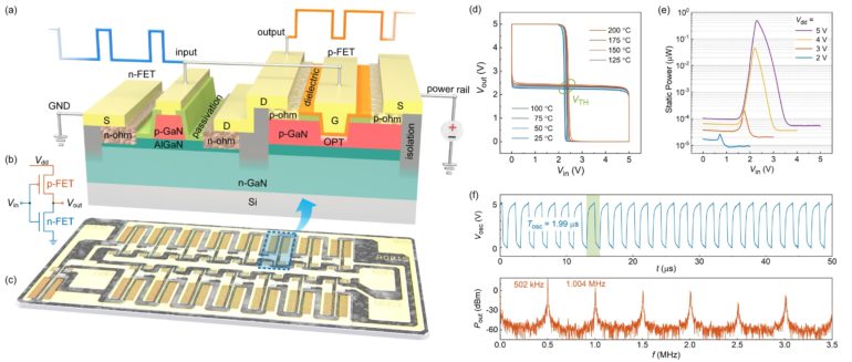
Researchers at the Hong Kong University of Science and Technology (HKUST) have recently realized a series of GaN-based complementary logic ICs. Their paper, published in Nature Electronics, could have important implications for the development of new types of electronics.
“Our work on GaN complementary logic integrated circuits (ICs) was carried out on a GaN-on-Si power HEMT (high-electron-mobility transistor) platform that currently dominates the mainstream commercial GaN power electronics device technology,” Prof. Kevin J. Chen, who led this study, told Tech Xplore. “This is a planar technology that is particularly suitable for the high-density integration of multi-functional blocks.”
To be efficient and complete, a power conversion system requires both core power switching devices, such as power transistors and rectifiers, and peripheral circuits that enable their driving, sensing, protective and control functionalities. Therefore, to unlock the full potential of GaN power HEMTs, enabling their high-frequency operation and the realization of smaller, more compact power systems, it would be preferable for power switching devices and peripheral circuits to be seamlessly integrated on a single chip.
“Current GaN HEMTs are all n-FETs with electrons as the carriers, thus all the peripheral circuits are also based on n-FETs,” Dr. Zheyang Zheng, one of the researchers who carried out the study, explained. “However, logic gates (which are a major constituent in the peripheral circuits) solely based on n-FETs, are much less energy-efficient than the well-known CMOS (complementary MOS) logic architecture that features complementary n-FETs and p-FETs.”
The main objective of the recent study was to develop GaN complementary or CMOS-like logic ICs that are compatible with existing GaN power HEMT platforms. Due to their advantages and wide bandgap, these ICs could benefit a wide range of technological applications, particularly those that are limited by the narrower bandgap of Si-based ICs.
“We demonstrate a suitable strategy to monolithically integrate GaN n-FETs and p-FETs and manifests the feasibility of constructing GaN-based complementary logic integrated circuits,” Zheng said. “Logic gates based on complementary n-FETs and p-FETs (i.e., the complementary logic gates) are the most energy efficient architectures for implementing digital logic circuits, as the use of complementary n-FETs and p-FETs results in substantially suppressed static power dissipation at both logic states (i.e., logic “1” and “0”), rail-to-rail input and output capability, well-placed logic transition threshold, and large noise margins.”
Using their fabrication strategy, Zheng and his colleagues demonstrated a full family of elementary logic gates, including NOT (inverter), NAND, NOR and transmission gates. In addition, as complex ICs require logic circuits featuring multiple stage logic gates, the team also demonstrated multi-stage digital ICs, such as a latch cell and ring oscillators, that can operate both at room temperature and at higher temperatures.
“Our study unambiguously manifests the feasibility of implementing GaN-based complementary logic circuits by demonstrating both a complete set of elementary logic gates and two multistage circuits,” Chen said. “Our findings imply that all GaN-based complementary logic circuits are technically within reach. Firstly, all building blocks are available. Secondly, they can be integrated together for more complex entities.”
To develop their GaN-based complementary circuits, the researchers used a commercial p-GaN gate power HEMT platform. The use of this commercial platform enables the integration of the complementary circuits they developed with existing power devices. As part of their study, the team also demonstrated the feasibility of this integration.
“As a first-generation demonstration with relatively large critical device dimension, our circuits can already work at sub-megahertz frequencies,” Zheng said. “It could be foreseen that moderate device downscaling and further improvement of the fabrication process would push the operating frequency to tens of megahertz, which would comfortably satisfy the requirements of currently used GaN-based power systems.”
The ICs that this team of researchers presented in their recent paper are based on a GaN p-channel FET technology they worked on for the past two years. Using a new oxygen plasma treatment technique, Zheng and his colleagues were able to simultaneously attain p-FET characteristics desirable for CMOS technology, including an enhancement-mode operation, low gate leakage, decent current density, and a high ON/OFF current ratio.
In the future, the ICs they created could aid the development of a wide range of technological devices, including tools for power conversion, oil well-logging, jet engine control and space exploration. Meanwhile, the researchers plan to investigate ways in which they could enhance their ICs further.
“We are going to work on down-scaling the devices, especially the p-channel transistors, for higher operating speed and lower power consumption,” Zheng added. “As these circuits are made on a commercial GaN-on-Si platform for manufacturing GaN power HEMTs, we would seek collaboration with the industry to deploy GaN complementary logic circuits in the peripheral circuits and integrate with the power HEMT for constructing more energy-efficient power conversion systems.”
Researchers realize vertical organic permeable dual-based transistors for logic circuits
More information:
Gallium nitride-based complementary logic integrated circuits. Nature Electronics(2021). DOI: 10.1038/s41928-021-00611-y.
2021 Science X Network
Citation:
Researchers realize gallium nitride-based complementary logic integrated circuits (2021, September 6)
retrieved 6 September 2021
from https://techxplore.com/news/2021-09-gallium-nitride-based-complementary-logic-circuits.html
This document is subject to copyright. Apart from any fair dealing for the purpose of private study or research, no
part may be reproduced without the written permission. The content is provided for information purposes only.


