It has been more than a decade since Gartner Research identified the Internet of Things—physical objects with sensors, processing ability and software that connect and exchange data through the Internet and communications networks—as an emerging technology.
Nowadays, connected devices are indispensable to commercial industries, health care and consumer products. Data analytics firm Statista forecasts a near tripling of the number of connected devices worldwide from 9.7 billion in 2020 to more than 29 billion in 2030.
The sensors embedded in devices are largely passive, transmitting signals to networked computers that process and return meaningful data to the device. Kyusang Lee, an assistant professor of materials science and engineering and electrical and computer engineering at the University of Virginia School of Engineering and Applied Science, is working on a way to make the sensors smart.
His smart sensor will sit at the edge of a device, which itself sits at the outer reaches of a wireless network. The smart sensor system also stores and processes data—an emerging area of research he calls artificial intelligence of things, a research strength of the Charles L. Brown Department of Electrical and Computer Engineering.
“Given the exponential growth in the Internet of Things, we anticipate data bottlenecks and lags in data processing and return signaling. The sensor’s output will be less reliable,” Lee said.
The constant pulsing of data through wireless and computer networks also eats up energy and increases the risk of exposing sensitive data to accidental or unauthorized disclosure and misuse.
Lee’s sensor system meets both of those challenges. An added benefit is that the sensor can detect and process a wide variety of signals that mimic human biology: image sensing for vision; ultrasound sensing for hearing; pressure sensing and strain detection tied to motion and touch; and chemical sensing to detect viruses.
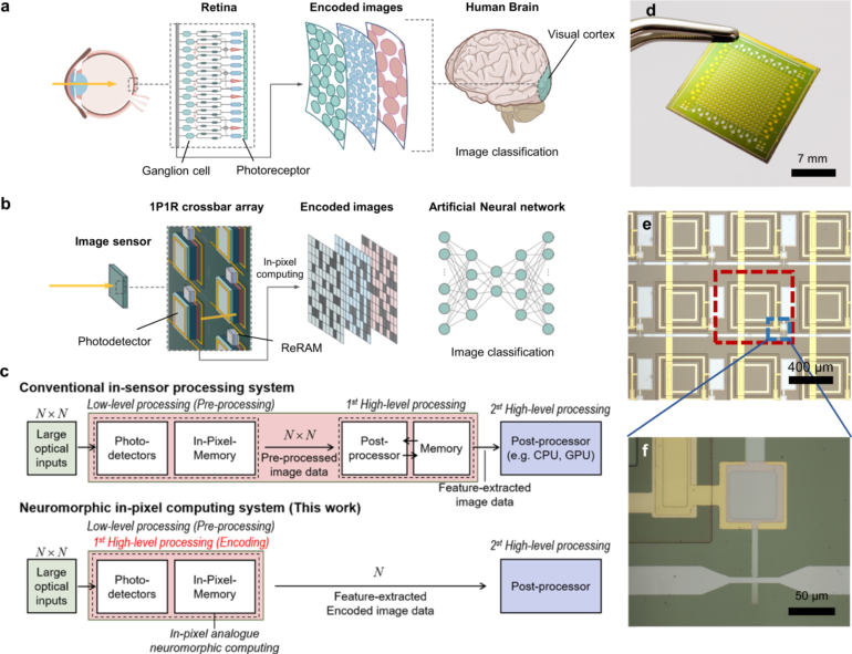
Lee and members of his thin-film device lab co-authored a paper in Nature Communications that points toward this holistic sensing system. In-sensor Image Memorization and Encoding via Optical Neurons for Bio-stimulus Domain Reduction Toward Visual Cognitive Processing is featured on the editor’s highlight page, earning recognition as one of the 50 best papers recently published in an area.
Lee’s sensor system culminates five years of research in electrical and optical materials development and device fabrication, a research strength of the Department of Materials Science and Engineering. His seminal research in epitaxy—the growth of a crystalline material on a 2D coated substrate—provides a new way to grow thin films.
Lee began this research as a postdoctoral associate in the Department of Mechanical Engineering at the Massachusetts Institute of Technology. Working with mechanical and electrical engineers and materials scientists at MIT, Lee developed a crystalline compound semiconductor growth process that overcame limitations imposed by lattice-matching between two material systems.
Lee commercialized his process, serving as chief executive officer and chief technology officer of a Charlottesville, Virginia start-up company FSB. The firm offers low-cost, large-scale, high-quality gallium nitride substrates for semiconductors commonly used in light-emitting diodes and enables clients to grow high-quality single crystalline semiconductors on graphene.
Lee’s innovation in materials synthesis, called remote epitaxy, enables fabrication of a high-quality, free-standing semiconductor film, meaning any given material layer can be designed with unique properties, independent of the material layers in which it is sandwiched. This flexibility in stacking the layers was a precursor step to fabricating a multi-functional sensor that can collect and simultaneously process different types of signal inputs.
The system’s optoelectronic component integrates image sensing and computing. Lee earned a prestigious National Science Foundation CAREER award to develop this smart image sensor system, which mimics the human eye. An artificial cornea and artificial iris perform basic optics, aided by artificial muscles that enable movement and focus. An artificial retina records the image signal, pre-processing the image data.
A software and hardware co-designed artificial neural network completes the sensor system. An artificial synapse, called the memristor, moves pre-processed sensory inputs to the brain of the system, a neuromorphic chip that can perform high-level signal processing.
“It is very satisfying to publish on systems integration,” Lee said. “We are now able to tell a complete story from materials to integration to application and present a vision for biomimicking sensor systems. I believe our sensor will be especially useful in robotics that rely on combined sensory inputs and real-time integrated processing.”
More information:
Doeon Lee et al, In-sensor image memorization and encoding via optical neurons for bio-stimulus domain reduction toward visual cognitive processing, Nature Communications (2022). DOI: 10.1038/s41467-022-32790-3
Provided by
University of Virginia
Citation:
Advances in in-sensor image memorization and encoding (2022, October 17)


