By using leaf skeletons as templates, researchers harnessed nature’s intrinsic hierarchical fractal structures to improve the performance of flexible electronic devices. Wearable sensors and electronic skins are examples of flexible electronics.
A research team at the University of Turku, Finland, has developed an innovative approach to replicating bioinspired microstructures found in plant leaf skeletons, eliminating the need for conventional cleanroom technologies. The work is published in the journal npj Flexible Electronics.
Fractal patterns are self-replicating structures in which the same shape repeats at increasingly smaller scales. They can be created mathematically and also occur in nature. For example, tree branches, leaf veins, vascular networks, and many floral patterns, such as cauliflower, follow a fractal structure.
Researchers created surfaces that mimic fractal patterns by utilizing dried tree leaf skeletons. Different manufacturing materials were sprayed onto the leaf skeletons, after which the new surfaces were separated from the leaf skeleton, and the researchers compared the structural properties and durability of the surfaces made from different materials.
This biomimetic surface, with more than 90% replication accuracy, is highly compatible with flexible electronic applications, offering enhanced stretchability, conformal attachment to skin, and superior breathability.
. © npj Flexible Electronics (2025). DOI: 10.1038/s41528-025-00381-z")
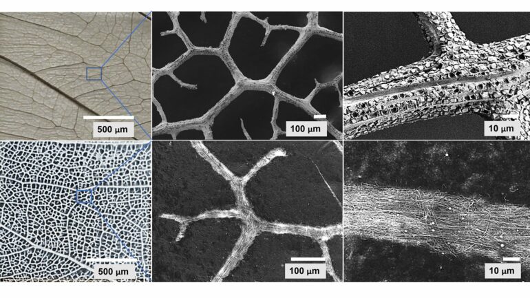
In the top row, close-up images of the leaf vein structure of the Ficus religiosa plant, and in the bottom row, close-up images of the biomimetic surface mimicking the leaf’s microstructures (made from Nylon 6 polymer). © npj Flexible Electronics (2025). DOI: 10.1038/s41528-025-00381-z
The advantages of surfaces based on fractal patterns are that their self-repeating hierarchical structures maximize the surface area while maintaining the surface’s mechanical flexibility. These unique patterns enhance the surface’s stretchability, and in electronic materials, the structure improves electrical conductivity, energy efficiency, energy dissipation, and charge transport.
These properties ensure durability and high performance under mechanical stress, making the surfaces ideal for next-generation flexible electronics, such as wearable sensors, transparent electrodes, and bioelectronic skin.
Compared to artificial fractals like kirigami or origami, leaf skeleton fractals offer naturally optimized, hierarchical, and scalable structures. They provide superior flexibility, breathability, and transparency while maintaining a high surface-area-to-volume ratio.
While leaf skeletons provide excellent fractal structures, they are not inherently stretchable, durable, or scalable due to their fixed dimensions and degradability. By replicating these patterns using stretchable and durable polymers using leaf skeletons as templates, researchers were able to create surfaces with enhanced flexibility and longevity, making large-scale production also feasible.
“We have succeeded in merging nature’s efficient designs with modern materials, which opens new possibilities for flexible and wearable electronics,” says Doctoral Researcher Amit Barua at the University of Turku.

A pressure sensor made from the surfaces mimicking the fractal structure of a leaf was directly mounted onto the fingertip of a robotic hand using encapsulation tape. This electronic skin allowed the robotic finger to sense touch, as the pressure sensor reacts to contact. This technology can also be used in prosthetic limb movement detection and human motion detection. © Timo Laukkanen
Reducing environmental impact
To make these biomimetic surfaces conductive, researchers applied a simple layer of metal nanowires, achieving a surface resistivity of approximately 20 Ω. These conductive surfaces were then integrated into applications such as tactile sensing, heating, and electronic skin devices.
This new biomimetic technique is more sustainable than traditional cleanroom-based methods, as it requires less energy and can be performed outside of controlled environments. The process can also use sustainable polymers, further reducing environmental impact.

For large-scale production, computer-aided design (CAD) models and finite element method (FEM) simulations can be used to replicate biotic designs with master collectors. Additionally, silver nanowires can be replaced with more sustainable conductive materials depending on the device’s requirements.
“To design sophisticated microstructures with high precision, cleanroom fabrication is usually required. This new biomimetic approach has the potential to bypass the need for cleanroom technologies when fabricating complex architectures, thereby contributing to lower carbon emissions,” says Barua.
More information:
Amit Barua et al, Biomimetic freestanding microfractals for flexible electronics, npj Flexible Electronics (2025). DOI: 10.1038/s41528-025-00381-z
Provided by
University of Turku
Citation:
Harnessing nature’s fractals for flexible electronics: Biomimetic fabrication technique uses leaf skeletons as templates (2025, March 24)