Researchers from UNSW Sydney have developed a tiny, transparent and flexible material to be used as a novel dielectric (insulator) component in transistors. The new material would enable what conventional silicon semiconductor electronics cannot do—get any smaller without compromising their function.
The research, recently published in Nature, indicates the potential for large-scale production of a 2D field-effect transistor—a device used to control current in electronics. The new material could help overcome the challenges of nanoscale silicon semiconductor production for dependable capacitance (electrical charge stored) and efficient switching behavior.
According to the researchers, this is one of the crucial bottlenecks to solve for the development of a new generation of futuristic electronic devices, from augmented reality, flexible displays and new wearables, as well as many yet-discovered applications.
“Not only does it pave a critical pathway to overcome the fundamental limit of the current silicon semiconductor industry in miniaturization, but it also fills a gap in semiconductor applications due to silicon’s opaque and rigid nature,” says Professor Sean Li, UNSW Materials and Manufacturing Futures Institute (MMFI) Director and principal investigator on the research. “Simultaneously, the elastic and slim nature could enable the accomplishment of flexible and transparent 2D electronics.”
Solving the semiconductor scaling issue
A transistor is a small semiconductive device used as a switch for electronic signals, and they are an essential component of integrated circuits. All electronics, from flashlights to hearing aids to laptops, are made possible by various arrangements and interactions of transistors with other components like resistors and capacitors.
As transistors have become smaller and more powerful over time, so too have electronics. Think your mobile phone—a compact hand-held computer with more processing power than the computers that sent the first astronauts to the moon.
But there’s a scaling problem. Developing more powerful future electronics will require transistors with sub-nanometer thickness—a size conventional silicon semiconductors can’t reach.
“As microelectronic miniaturization occurs, the materials currently being used are pushed to their limits because of energy loss and dissipation as signals pass from one transistor to the next,” says Prof. Li.
Microelectronic devices continue to diminish in size to achieve higher speeds. As this shrinkage occurs, design parameters are impacted in such a way that the materials currently being used are pushed to their limits because of energy loss and dissipation as signals pass from one transistor to the next. The current smallest transistors made of silicon-based semiconductors are 3 nanometers.
To get an idea of just how small these devices need to be—imagine one centimeter on a ruler and then count the 10 millimeters of that centimeter. Now, in one of those millimeters, count another one million tiny segments—each of those is one nanometer or nm.
“With such limits, there has been an enormous drive to radically innovate new materials and technologies to meet the insatiable demands of the global microelectronics market,” says Prof. Li.

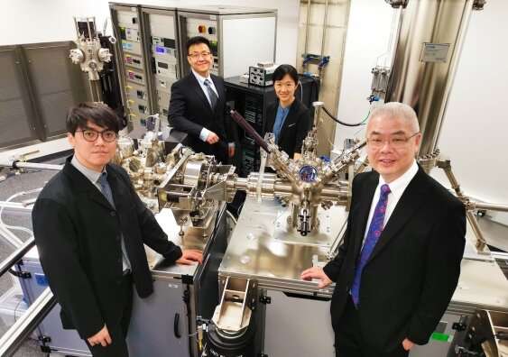
Dr Jing-Kai Huang, Dr Ji Zhang, Dr Junjie Shi and Professor Sean Li from the UNSW Materials and Manufacturing Futures Institute. © Robert Largent
Breaking the bottleneck for future electronics
For the research, MMFI engineers fabricated the transparent field-effect transistors using a freestanding single-crystal strontium titanate (STO) membrane as the gate dielectric. They discovered their new miniaturized devices matched the performance of current silicon-semiconductor field-effect transistors.
“The key innovation of this work is that we transformed conventional 3D bulk materials into a quasi-2D form without degrading its properties,” says Dr. Jing-Kai Huang, the paper’s lead author. “This means it can be freely assembled, like LEGO blocks, with other materials to create high-performance transistors for a variety of emerging and undiscovered applications.”
The MMFI academics drew on their diverse expertise to complete the work.
“Fabricating devices involves people from different fields. Through MMFI, we have established connections with academics who are experts in the 2D electric device fields as well as the semiconductor industry,” says Dr. Ji Zhang, a co-author of the paper.
“The first project was to fabricate the freestanding STO and to study its electrical properties. As the project progressed, it evolved into fabricating 2D transistors using freestanding STO. With the help from the platform established by MMFI, we were able to work together to finish the project.”
The team is now working towards wafer-scale production. In other words, they hope to see whether the material can be used to build all the circuits for an entire computer on one chip.
“Extensive data sets were collected to support the performance of these 2D electronics, indicating the technology’s promise for large-size wafer production and industrial adoption,” says Dr. Junjie Shi, another co-author of the paper.
“Achieving this will enable us to fabricate more complex circuits with a density closer to commercial products. This is the crucial step to make our technology reach people,” says Dr. Huang.
The researchers also say their development is a promising step toward a new era of electronics and local manufacturing resilience.
“From shifting geopolitics and the pandemic, we have seen more disruption in the global semiconductor supply chain, and we believe this is also an opportunity for Australia to join and strengthen this supply chain with our unique technology in the near future,” Dr. Huang says.
Currently, the technology is protected by two Australian provisional patent applications, with MMFI and UNSW looking to commercialize the intellectual property and bring it to market.
“We are currently fabricating logic circuits with the transistors,” says Prof. Li. “At the same time, we are approaching several leading industries in the Asia-Pacific region to attract investment and establish a semiconductor manufacturing capability in NSW via industrialisation of this technology.”
More information:
Jing-Kai Huang et al, High-κ perovskite membranes as insulators for two-dimensional transistors, Nature (2022). DOI: 10.1038/s41586-022-04588-2
Provided by
University of New South Wales
Citation:
Engineers develop new integration route for tiny transistors (2022, August 3)


