The invention of the transistor by Bell Laboratory in 1947 ushered in an era of electronic devices that were smaller and ran cooler using far less power than their bulky and fragile vacuum tube counterparts. Transistors function as a binary switch to facilitate electrical current from off to on states. Radios, calculators and telephones were among the first wave of instruments to replace vacuum tubes with the new semiconductor technology. As the technology scaled smaller and smaller, subsequent decades saw the steady integration of silicon transistors into devices, and today’s computers, cell phones, watches, pacemakers, and virtually every kind of electronic device relies on them for high-speed processing and memory.
Enter the memristor, an electronic device that emulates the binary switch using a two- and also three-dimensional matrix configuration, or cross bar array, to regulate states of conductivity based on current resistance. Dr. Mario Lanza, KAUST associate professor of material science and engineering, asserts that, like the transistor, it’s only a matter of time before memristors become the new switching technology standard, surpassing transistors in speed and operational efficiency.
Lanza is the lead author of a recently published review paper, Memristive technologies for data storage, computation, encryption, and radio-frequency communication, as part of Science magazine’s coverage of the 75th anniversary of the discovery of the transistor. With contributed findings by co-authors from both industry and academia, the paper is the first to provide a comprehensive summary of data that supports memristor technology readiness level across materials and applications.
“Memristors can primarily be made from four different materials that can be applied to four applications, for a total of 16 combinations, and this paper covers them all,” said Lanza. “We statistically show the technical criteria for how memristors function in these various configurations. You see what works, which is very exciting. Our compilation of findings can have an important impact on the field.”
Lanza foresees that in the future, many other combinations may be possible because memristors made of two-dimensional layered materials and perovskites are improving their performance quickly, and additional applications may be designed.
Going beyond
Current chip technology has already reached the fundamental quantum mechanics limit in terms of size. Chip transistors can’t get smaller than the interatomic distance. Since scaling down isn’t an option, memristive technology scales up, integrating vertical, three-dimensional technology involving a nano-sized matrix of metallic wires with an insulating switch—the memristor—at every junction. Applying voltage pulses breaks the insulation, creating a path for current flow. In removing the voltage, the modified structure of the material remains as a conductive ghost, or memory that, when voltage is applied again, can be reversed to recover the initial state.
In this way the memristor serves as a polarity switch that can be toggled between conductive and non-conductive states. Lanza said this capability can be used for many different functions within an integrated sequence.

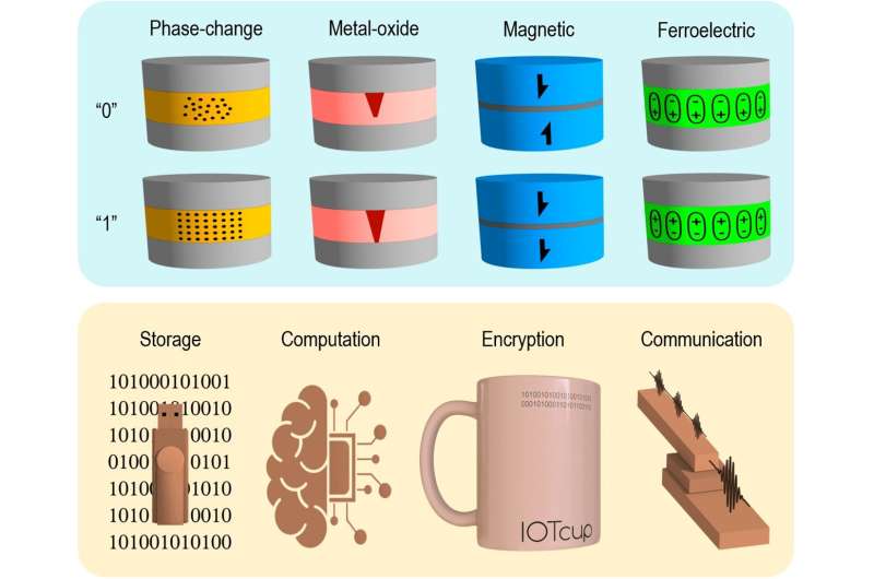
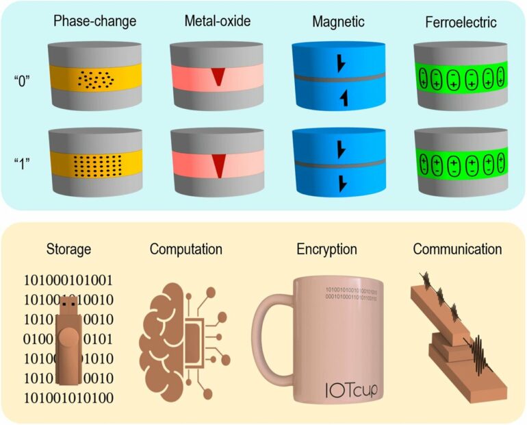
Memristive devices, in which electrical resistance can be adjusted to two or more nonvolatile levels, can be fabricated using different materials (top row). This allows adjusting their performance to fulfill the requirements of different technologies. Memristive memories are a reality, and important progress is being achieved in advanced computation, security systems, and mobile communication (bottom row). © King Abdullah University of Science and Technology
“The memristor is like a Swiss Army knife. It can be used for many things,” Lanza said. “It’s a switch with many states that I can adjust, whether I want 25 stable or unstable states, or ten or two. The grid can be programmed to make advanced computations at rapid speeds, consuming far less energy in far less space and across more applications—calculations that would otherwise require many transistors to do the same job.”
The four kinds of non-silicon-based materials that Lanza said are being used to make memristors are metal-oxides, such as hafnium dioxide; phase-change, i.e.,chalcogens; magnetic, i.e., cobalt or iron; and ferroelectric, i.e., barium titanate. The primary applications for which memristors are used are storage, computation, communication and encryption. Based on the material used and the electrical resistance applied, performance can be adjusted to meet the requirements of different technologies.
Addressing the gaps
The 3D integration of memristors allows more devices to be packed while maintaining the smallest size possible, proving that size isn’t the holy grail of operational excellence. Lanza said this technology is already being done with transistors, but it’s new terrain for memristors. Even though the concept of memristors was introduced in the 1970’s, the technology hasn’t made traction until the last decade or so.
Whereas memristors can already be found in some products, such as data centers and watches, Lanza said there are many promising applications yet to explore, and that industry is closely tracking the technology to assess future commercial uses beyond silicon transistor electronics.
He credits the scope and detail of the paper’s findings to the cross-disciplinary nature of the team. Three of the co-authors are scientists from industry, and six, including Lanza, from academia. Of the three authors from industry, one is from Taiwan Semiconductor Manufacturing Company (TSMC)—the multinational company responsible for producing most of the chips in the world, including the smallest and most advanced microchips; and two are from International Business Machines (IBM)—a leader in providing advanced information technology, with operations in more than 170 countries.
The paper’s contributing authors from academia bring expertise in specific memristor applications, including data encryption, an area where information for industry standards has been lacking. Lanza said the paper addresses these gaps, establishing a baseline of technical specification standards that industries and others can reference and refine.
With market forecasts expected to grow up to $5.6 billion dollars by 2026—a 2% gain in the nearly $280 billion memory market—he hopes the paper will give companies the incentive needed to invest in new memristor-based technologies.
Dr. Meng-Fan Chang, Director of Corporate Research at TSMC and Distinguished Professor at National Tsing Hua University, said, “This is the first article that provides a wide overview about the structure and applications of memristors—the electronics device that is expected to revolutionize the microelectronics industry.”
More information:
Mario Lanza et al, Memristive technologies for data storage, computation, encryption, and radio-frequency communication, Science (2022). DOI: 10.1126/science.abj9979
Provided by
King Abdullah University of Science and Technology
Citation:
From transistor to memristor: Switching technologies for the future (2022, June 28)


