With brilliant colors and picturesque shapes, many crystals are wonders of nature. Some crystals are also wonders of science, with transformative applications in electronics and optics. Understanding how best to grow such crystals is key to further advances.
Scientists from the U.S. Department of Energy’s (DOE) Argonne National Laboratory, along with three universities, have revealed new insights into the mechanism behind how gallium nitride crystals grow at the atomic scale.
Gallium nitride crystals are already in wide use in light-emitting diodes, better known as LEDs. They might also be applied to form transistors for high-power switching electronics to make electric grids more energy efficient and smarter. The use of such “smart grids,” which could better balance high power within the overall system, might prevent people from losing power in severe storms.
“This work is a great example of the importance and power of probing a material while a process is underway. Quite often when we use such probes to study processes like synthesis, we find the story to be more complex than we originally thought and counter to conventional wisdom.”—Matt Highland, X-ray Sciences division, Argonne National Laboratory
The same technology could also make individual homes more energy efficient. And it could find use in optical communications, where lasers transmit information. Such information transfer can be more precise, faster and more secure than current capabilities.
Because of these diverse applications, scientists worldwide have been working to improve the process for growing gallium nitride crystals.
“Gallium nitride has a more complicated crystal structure than silicon, the typical crystalline material in electronics,” said G. Brian Stephenson, an Argonne distinguished fellow in the Materials Science division. “When you grow this crystal, you thus get more fascinating behavior at the surface.”
At the atomic scale, a growing gallium nitride crystal surface typically looks like a staircase of steps, where every stair is a layer of the crystal structure. Atoms are added to a growing crystal surface by attachment at the edges of the steps. Because of the gallium nitride crystal structure, the steps have alternating edge structures, labeled A and B. The different atomic structures lead to different growth behaviors of the A and B steps. Most theoretical models indicate that atoms accumulate faster on a B-type step, but experimental confirmation has been lacking.
“Because of the high temperatures and chemical atmosphere involved, it is not possible to examine the growth of gallium nitride with a standard electron microscope and test the model prediction,” Stephenson said. For that, the team called upon the Advanced Photon Source (APS), a DOE Office of Science User Facility at Argonne.
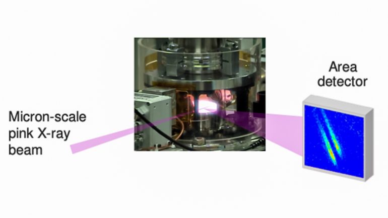
The very high energy of the X-rays available at the APS with a beam only a few micrometers wide (beamline 12-ID-D) allowed the team to monitor the rate of gallium nitride growth on the crystal surface steps. These X-rays are an ideal probe since they are sensitive to atomic-scale structure and can penetrate the environment of the crystal at the high temperatures involved, over 1400 degrees Fahrenheit, while it is growing.
“Based on modeling, many had assumed that atoms probably build up faster on the type-B step,” Stephenson said. “Imagine our surprise when it turned out to be step A. This suggests the chemistry of the growth process may be more complicated than previously thought.”
“This work is a great example of the importance and power of probing a material while a process is underway,” added Matt Highland, physicist in the X-ray Sciences division. “Quite often when we use such probes to study processes like synthesis, we find the story to be more complex than we originally thought and counter to conventional wisdom.”
The results have obvious implications for refining the current understanding of the atomic-scale mechanisms of gallium nitride growth. This understanding has important practical implications for design of advanced gallium nitride devices by allowing better control of growth and incorporation of additional elements for improved performance. The findings can also be applied to growth of related crystals, including host semiconductor materials for quantum information science.
This research was supported by the DOE Office of Basic Energy Sciences. It was reported in Nature Communications, in a paper titled “In situ microbeam surface X-ray scattering reveals alternating step kinetics during crystal growth.” In addition to Stephenson and Highland, other Argonne authors include Guangxu Ju, Dongwei Xu (now at Huazhong University of Science and Technology), Eastman and Peter Zapol. University participants include Carol Thompson (Northern Illinois University) and Weronika Walkosz (Lake Forest College).
Development of a new technique for growing high-quality gallium nitride crystals
More information:
Guangxu Ju et al, In situ microbeam surface X-ray scattering reveals alternating step kinetics during crystal growth, Nature Communications (2021). DOI: 10.1038/s41467-021-21927-5
Provided by
Argonne National Laboratory
Citation:
Unveiling what governs crystal growth (2021, May 27)
retrieved 27 May 2021
from https://phys.org/news/2021-05-unveiling-crystal-growth.html
This document is subject to copyright. Apart from any fair dealing for the purpose of private study or research, no
part may be reproduced without the written permission. The content is provided for information purposes only.


