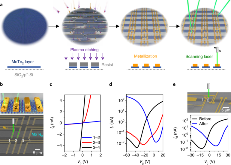
For decades, transistors—the heart of computer chips—have been getting smaller and smaller. As a result, the electronic components in many devices can be made even more compact, faster and also more powerful. But is this development coming to a natural halt? The smaller the components, the greater the danger that individual defects in the atomic structure will significantly change the behavior of the component. This applies to the established silicon technology and novel nanotechnologies based on 2D materials.
At Vienna University of Technology (TU Wien), intensive work has been done on the physical description of this problem at the transistor level. Now the researchers are going a step further and looking at the influence of defects at the level of electronic circuits, which sometimes consist of several—sometimes even billions—of transistors. In some cases, individual transistors can operate outside the desired specification, but still perform well as part of a circuit consisting of several transistors. With this new approach at the circuit level, significant advances in miniaturization are still possible.
The study is published in the journal Advanced Materials.
Smaller components, bigger errors
“The smallest transistors today are only a few nanometers in size,” says Michael Waltl from the Institute for Microelectronics at TU Wien. “So one has advanced to the atomic scale.” But transistors are never perfect at the atomic level: Sometimes an atom may be in the wrong place, and sometimes the connection between two different crystals is not quite exact.
“In larger components, such errors do not play such a dominant [role]. But with tiny transistors in the order of a few nanometers, even a single defect can lead to the transistor’s characteristic curves being far outside the specified tolerance range. Thus, it is considered unusable,” Waltl continues.
The effect of material defects in electronic components is usually recorded statistically in the industry: Tens of thousands of transistors are manufactured and measured. Based on the variability determined in this way, one can then calculate whether these transistors are usable or whether one must adjust the geometry or production process and reduce the number of defects. In the worst case, one would then have to increase the area of the chip, for example. This can hurt the chip’s performance and increase its price.
“Just looking for transistors with properties outside the desired parameter range is an oversimplified view,” says Waltl. “After all, the transistors are connected to form an electronic circuit—for example, an inverter that inverts a signal or memory consisting of six transistors. The interesting question is not whether a single transistor meets certain abstract criteria when faults occur at the atomic level, but whether the entire circuit behaves correctly.”
The microelectronics team at TU Wien approached this question with a combination of experiments and computer simulations. Numerous electronic components were examined, and elaborate computer models were created based on the results.
Precise computer models make it possible to design robust circuits
It turns out that even transistors with errors are not necessarily useless. “The fault tolerance depends on the circuit—which should be considered when designing the circuits,” says Waltl. “It may be, for example, that the transistor must be particularly low-fault at a particular point in the electronic circuit but that the tolerances are greater for another transistor in the same circuit.” In such a case, two different types of transistors could be used to ensure that the circuit performs its task reliably.
“Our results apply to silicon transistors and novel 2D semiconductors,” Waltl clarifies. “Whatever technology you want to use to create the next generation of chips with even smaller components: In any case, the effect of unavoidable errors should not only be described empirically, as has been the case up to now, but one should resort to advanced physical computational models to simulate partial circuits or entire circuits to get the best out of the new possibilities.”
More information:
Michael Waltl et al, Perspective of 2D Integrated Electronic Circuits: Scientific Pipe Dream or Disruptive Technology?, Advanced Materials (2022). DOI: 10.1002/adma.202201082
Provided by
Vienna University of Technology
Citation:
Examining the influence of defects on 2D integrated electronic circuits (2023, January 16)


