Ferroelectric semiconductors are contenders for bridging mainstream computing with next generation architectures, and now a team at the University of Michigan has made them just five nanometers thick—a span of just 50 or so atoms.
This paves the way for integrating ferroelectric technologies with conventional components used in computers and smartphones, expanding artificial intelligence and sensing capabilities. They could also enable batteryless devices, crucial for the Internet of Things (IoT) that powers smart homes, identifies problems with industrial systems and alerts people to safety risks, among other things.
The study in Applied Physics Letters was selected as an editor’s pick.
“This will allow the realization of ultra-efficient, ultra-low-power, fully integrated devices with mainstream semiconductors,” said Zetian Mi, U-M professor of electrical and computer engineering and co-corresponding author of the study. “This will be very important for future AI and IoT-related devices.”
Ferroelectric semiconductors stand out from others because they can sustain an electrical polarization, like the electric version of magnetism. But unlike a fridge magnet, they can switch which end is positive and which is negative. This property can be used in many ways—including sensing light and acoustic vibrations, as well as harvesting them for energy.
“These ferroelectric devices could be self-powered,” Mi said. “They can harvest ambient energy, which is very exciting.”
And they offer a different way of storing and processing both classical and quantum information. For instance, the two electrical polarization states can serve as the one and zero in computing. This way of computing can also emulate the connections between neurons, which enable both memory storage and information processing in the brain. Known as neuromorphic computing, this kind of architecture is ideal for supporting AI algorithms that process information through neural networks.
Storing energy as electrical polarization requires less energy than the capacitors in RAM, which constantly draw power or else lose the data they store, and could even outlast an SSD. This kind of memory could be more densely packed, increasing capacity, as well as being more robust to harsh environments including extreme temperatures, humidity and radiation.
Mi’s team had previously demonstrated ferroelectric behavior in a semiconductor made of aluminum nitride spiked with scandium, a metal sometimes used to fortify aluminum in performance bicycles and fighter jets. However, to use it in modern computing devices, they needed to be able to make it in films thinner than 10 nanometers, or about the thickness of 100 atoms.

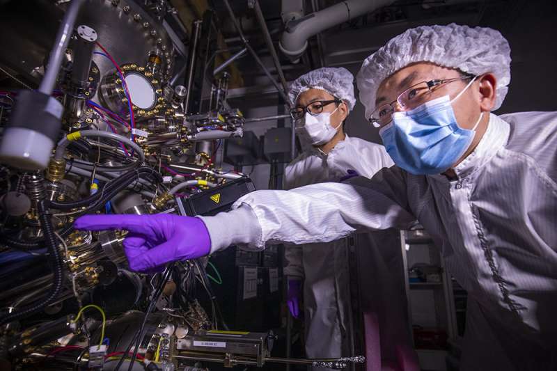
ECE Research Scientists Ding Wang and Ping Wang discuss the growth behavior of single-crystalline ferroelectric scandium aluminum nitride (ScAlN) deposited using a molecular beam epitaxy system inside Professor Zetian Mi’s lab on North Campus in Ann Arbor, MI, May 14th, 2021. © Robert Coelius, University of Michigan
They achieved this with a technique called molecular beam epitaxy, the same approach used to make semiconductor crystals that drive the lasers in CD and DVD players. In a machine with strong steampunk vibes, they were able to lay down a crystal 5 nanometers thick—the smallest scale ever achieved. They did this by precisely controlling every layer of atoms in the ferroelectric semiconductor, as well as minimizing the losses of atoms from the surface.
“By reducing the thickness, we showed that there is a high possibility that we can reduce the operation voltage,” said Ding Wang, a research scientist in electrical and computer engineering and first author of the study. “This means we can reduce the size of the devices and reduce the power consumption during operation.”
In addition, the nanoscale manufacturing improves the researchers’ ability to study the fundamental properties of the material, discovering the limits of its performance at small sizes, and possibly opening the way to its use in quantum technologies due to its unusual optical and acoustic properties.
“With this thinness, we can really explore the miniscule physics interactions,” said Ping Wang, U-M research scientist in electrical and computer engineering. “This will help us to develop future quantum systems and quantum devices.”
More information:
Ding Wang et al, Thickness scaling down to 5 nm of ferroelectric ScAlN on CMOS compatible molybdenum grown by molecular beam epitaxy, Applied Physics Letters (2023). DOI: 10.1063/5.0136265
Provided by
University of Michigan
Citation:
Nanoscale ferroelectric semiconductor could power AI and post-Moore’s Law computing on a phone (2023, February 6)


