Big Blue has unveiled Telum, its first chip with AI inferencing acceleration that will allow it to conduct tasks such as fraud detection while a transaction is occurring.
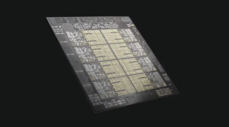
“The chip contains 8 processor cores with a deep super-scalar out-of-order instruction pipeline, running with more than 5GHz clock frequency, optimised for the demands of heterogenous enterprise-class workloads,” IBM said.
“The completely redesigned cache and chip-interconnection infrastructure provides 32MB cache per core, and can scale to 32 Telum chips. The dual-chip module design contains 22 billion transistors and 19 miles of wire on 17 metal layers.”
The chip was built on 7nm extreme ultraviolet technology created by Samsung, and represents the initial involvement of the IBM Research AI Hardware Center.
In development for three years, the first system using the chip is slated for the first half of 2022.
Senior technical staff member for IBM Z hardware development Anthony Saporito said the L2 caches can combine and form a virtual 256MB L3 cache, and up to eight Telum chips could combine to form a virtual 2GB L4 cache.
“One of the key innovations here on the Telum design is, we built an AI accelerator right onto the silicon of the chip and we directly connected all of the cores and built an ecosystem up the stack, through the hardware design, through firmware, and through the operating systems, and the software that enables bringing this deep learning into transactions, all of the transactions,” he said.
“That part of the design is a really cool collaborative design that we did between the research group and the systems group, and that directly connected design built for deep learning inferencing allows us to run at scale.

“Those thousands and thousands of transactions per second … with this technology are able to do real-time deep learning inferencing, fraud detection, and analytics and gain insights as those transactions are running at the system and they’re able to do that at scale and with all of the reliability and zero downtime, that’s critical to this platform.”
In May, IBM Research created a test semiconductor with 2nm fabrication that Big Blue claimed would improve performance by 45% using the same amount of power or use 75% less energy when compared to 7nm-based chips.
The 2nm technology will go into production toward the end of 2024. Mass usage could come around 2025.
“This is exciting because most advanced manufacturing in the world is in about 7nm and some are in 5mn, and we are here to show we could put together a 2nm transistor. That means this industry will keep going for the next decade, that’s what these results mean,” IBM Research vice president Mukesh Khare said at the time.