A group of international researchers at The University of Manchester have revealed a novel method that could fine tune the angle—”twist”—between atom-thin layers that form exotic manmade nanodevices called van der Waals heterostructures—and help accelerate the next generation of electronics.
The new technique can achieve in situ dynamical rotation and manipulation of 2-D materials layered on top of each other to form van der Waals heterostructures—nanoscale devices that boast unusual properties and exciting new phenomena, explained team leader Professor Mishchenko.
Tuning of twist angle controls the topology and electron interactions in 2-D materials—and such a process, referred to as ‘twistronics’, is a rising research topic in physics in recent years. The new Manchester-led study will be published in Science Advances today.
“Our technique enables twisted van der Waals heterostructures with dynamically tuneable optical, mechanical, and electronic properties.” explained Yaping Yang, the main author of this work.
Yaping Yang added: “This technique, for example, could be used in autonomous robotic manipulation of two-dimensional crystals to build van der Waals superlattices, which would allow accurate positioning, rotation, and manipulation of 2-D materials to fabricate materials with desired twist angles, to fine-tune electronic and quantum properties of van der Waals materials.”
Twisting layers of 2-D crystals with respect to each other results in the formation of a moiré pattern, where lattices of the parent 2-D crystals form a superlattice. This superlattice can completely change the behaviour of electrons in the system, leading to observation many novel phenomena, including strong electron correlations, fractal quantum Hall effect, and superconductivity.
The team demonstrated this technique by successfully fabricating heterostructures where graphene is perfectly aligned with both top and bottom encapsulating layers of hexagonal boron nitride—dubbed “white graphene”—creating double moiré superlattices at the two interfaces.
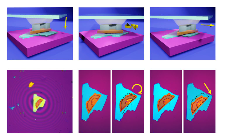
As published in Science Advances, the technique is mediated by a polymer resist patch on target 2-D crystals and a polymer gel manipulator, which can precisely and dynamically control the rotation and positioning of 2-D materials.
“Our technique has the potential to bring twistronics inside cryogenic measurement systems, for instance, by using micromanipulators or micro-electro-mechanical devices” added Artem Mishchenko.
The researchers used a glass slide with a droplet of polydimethylsiloxane (PDMS) as a manipulator, which is cured and naturally shaped into a hemisphere geometry. In the meantime, they intentionally deposited an epitaxial polymethyl methacrylate (PMMA) patch on top of a target 2-D crystal through a standard electron-beam lithography.
The steps to manipulate target flakes in a heterostructure is easy to follow. By lowering down the polymer gel handle, PDMS hemisphere is brought in contact with the PMMA patch. When they touch each other, one can easily move or rotate the target 2-D crystals on the surface of the bottom flake. Such a smooth movement of the 2-D flakes is based on the superlubricity between the two crystalline structures.
Superlubricity is a phenomenon where the friction between atomically flat surfaces disappears depending on certain conditions.
The manipulation technique enables continuous tuning of the twist angle between the layers even after the heterostructure assembly. One can design the epitaxial PMMA patch into an arbitrary shape on demand, normally taking the geometry that fits the target flake. The manipulation technique is convenient and reproducible since the PMMA patch can be easily washed away by acetone and re-patterned by lithography.
Normally, for a carefully fabricated PDMS hemisphere, the contact area between the hemisphere and a 2-D crystal depends on the hemisphere radius and is highly sensitive to the contact force, making it difficult to precisely control the motion of the target 2-D crystal.
“The epitaxial PMMA patch plays a crucial role in the manipulation technique. Our trick lies in that the contact area of the polymer gel manipulator is limited precisely to the patterned shape of the epitaxial polymer layer. This is the key to realize precise control of the manipulation, allowing a much larger controlling force to be applied.” said Jidong Li, one of the co-authors.
Compared to other manipulation techniques of 2-D materials, such as using atomic force microscope (AFM) tips to push a crystal with a specifically fabricated geometry, the in situ twistronics technique is non-destructive and can manipulate flakes regardless of their thickness, whereas an AFM tip works better only for thick flakes and might destroy thin ones.
Perfect alignment of graphene and hexagonal boron nitride demonstrates the potential of the technique in twistronics applications.
Using the in-situ technique, the researchers successfully rotated 2-D layers in a boron nitride/graphene/boron nitride heterostructure to realize a perfect alignment between all the layers. The results demonstrate the formation of double moiré superlattices at the two interfaces of the heterostructure. In addition, the researchers observed the signature of the second-order (composite) moireacute; pattern generated by the double moireacute; superlattices.
This heterostructure with perfectly aligned graphene and boron nitride demonstrates the potential of the manipulation technique in twistronics.
“The technique can be easily generalized to other 2-D material systems and allows for reversible manipulation in any 2-D systems away from commensurate regime”, said Yaping Yang, who carried out the experimental work.
Professor Mishchenko added: “We believe our technique will open up a new strategy in device engineering and find its applications in research of 2-D quasicrystals, magic-angle flat bands, and other topologically nontrivial systems.”
Abnormal conductivity in low angle twisted bilayer graphene
More information:
“In situ manipulation of Van der Waals heterostructures for twistronics” Science Advances (2020). advances.sciencemag.org/lookup … .1126/sciadv.abd3655
Provided by
University of Manchester
Citation:
Fine tuning the “twist” between 2-D materials in van der Waals heterostructures to help accelerate next gen electronics (2020, December 4)
retrieved 4 December 2020
from https://phys.org/news/2020-12-fine-tuning-d-materials-van.html
This document is subject to copyright. Apart from any fair dealing for the purpose of private study or research, no
part may be reproduced without the written permission. The content is provided for information purposes only.