
A group of photonics researchers at Tampere University have introduced a novel method to control a light beam with another beam through a unique plasmonic metasurface in a linear medium at ultra-low power. This simple linear switching method makes nanophotonic devices such as optical computing and communication systems more sustainable, requiring low intensity of light.
All-optical switching is the modulation of signal light due to control light in such a way that it possesses the on/off conversion function. In general, a light beam can be modulated with another intense laser beam in the presence of a nonlinear medium.
The switching method developed by the researchers is fundamentally based on the quantum optical phenomenon known as Enhancement of Index of Refraction (EIR).
“Our work is the first experimental demonstration of this effect on the optical system and its utilization for linear all-optical switching. The research also enlightens the scientific community to achieve loss-compensated plasmonic devices operating at resonance frequencies through extraordinary enhancement of refractive index without using any gain media or nonlinear processes,” says Humeyra Caglayan, Associate Professor (tenure track) in Photonics at Tampere University.
Optical switching enabled with ultrafast speed
High-speed switching and low-loss medium to avoid the strong dissipation of signal during propagation are the basis to develop integrated photonic technology where photons are utilized as information carriers instead of electrons. To realize on-chip ultrafast all-optical switch networks and photonic central processing units, all-optical switching must have ultrafast switching time, ultralow threshold control power, ultrahigh switching efficiency, and nanoscale feature size.
“Switching between signal values of 0 and 1 is fundamental in all digital electronic devices including computers and communication systems. Over the past decades, these electronic elements have gradually become smaller and faster. For example, the ordinary calculations done with our computers on the order of seconds could not be done with old room-sized computers, even in several days,” Caglayan remarks.
In conventional electronics, switching relies on controlling the flow of electrons on the time scale of a microsecond (10-6 sec) or nanosecond (10-9 sec) range by connecting or disconnecting electrical voltage.
“However, the switching speed can be raised to an ultrafast time scale (femtosecond 10-15 sec) by replacing the electrons with plasmons. Plasmons are a combination of photons and a collection of electrons on the surface of metals. This enables optical switching with our device with femtosecond (10-15 sec) speeds,” she states.
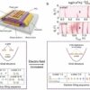
“Our plasmonic nano-switch consists of an L-shaped combination of metallic nanorods. One of the nanorods receives a linearly polarized signal and the other receives another linearly polarized ‘control’ beam perpendicular to the first beam,” says Postdoctoral Research Fellow Rakesh Dhama, the first author of the article published in Nature Communications.
Polarization means the direction in which the electric field of the beam is oscillating. The control beam can attenuate or amplify the signal depending on the phase difference between the beams. The phase difference refers to the time difference when each beam reaches its maximum intensity. The signal amplification occurs due to the transfer of some optical energy from the control beam to the signal through a constructive superposition with a carefully engineered phase difference.
Enhancing the performance of plasmonic devices
Similarly, the attenuation of the signal is achieved by destructive superposition when the beams have the opposite phase difference. This finding makes nanophotonic devices such as optical computing and communication systems more sustainable requiring low intensity of light. This simple linear switching method can replace the current methods of optical processing, computing, or communication by accelerating the development and realization of nanoscale plasmonic systems.
“We expect to see further studies of plasmonic structures utilizing our improved switching method and possibly the use of our method in plasmonic circuits in the future. Additionally, the L-shaped metasurface could be further studied to reveal ultrahigh-speed switching under the illumination of femtosecond laser pulses and to investigate the nonlinear enhancement and control of plasmonic nanoparticles,” Humeyra Caglayan notes.
Controlling the nonlinear response of nanostructures provides even more interesting applications and functionalities to nanophotonic devices such as optical computing and communication systems.
“This approach has also the potential to enhance the performance of plasmonic devices by creating broadband transparency for a signal beam without any gain medium. It can open up several ways to design smart photonic elements for integrated photonics,” Cagalayan says.
More information:
Rakesh Dhama et al, All-optical switching based on plasmon-induced Enhancement of Index of Refraction, Nature Communications (2022). DOI: 10.1038/s41467-022-30750-5
Provided by
Tampere University
Citation:
A novel all-optical switching method makes optical computing and communication systems more power-efficient (2022, June 6)