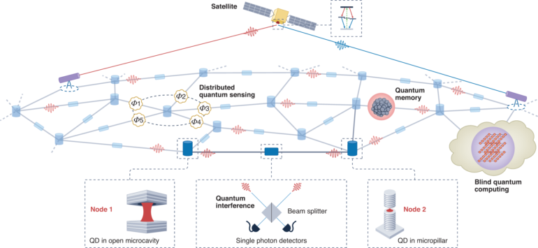
Scientists from The Institute of Scientific and Industrial Research (SANKEN) at Osaka University, in collaboration with the Canadian National Research Council (NRC), developed a gallium arsenide (GaAs) quantum dot that can trap individual electrons. By controlling the crystallographic orientation of the substrate, the research team hopes to optimize the conversion of photons into spin-polarized electrons. This work may help make quantum networks more practical, especially for encrypting secure data.
Every computer or tablet you have owned is based on computations using the charge of electrons. While current electronic devices have achieved amazing feats of processing speed while becoming ever smaller, there is the possibility that manufacturers may someday soon come up on fundamental limits of what can be done using conventional methods. A promising alternative is to also use the intrinsic magnetic moment of electrons, called “spin.” Because these spins can be put into a superposition of both up and down simultaneously, it opens the way for quantum computers that may be able to solve certain problems much faster than current hardware. Spin can be also used as the medium for quantum communication by transferring quantum information with light. But this process of transferring information to the spin of extremely small electrons is challenging and has to be performed efficiently.
Now, a team of researchers led by Osaka University have realized the world’s first GaAs gate-controlled quantum dot circuit on a (110)-oriented surface that promises to increase photon-electron spin conversion efficiency (see Fig.1). This has the effect of encoding quantum information from incident photons into the electron spins. “We believe our research is the first demonstration of a gate-defined quantum dot circuit that also has charge detection capabilities, using this particular orientation of a GaAs substrate,” first author Tomohiro Nakagawa says.
Photon-electron spin conversion is performed by exciting an electron and a hole via absorption of a photon. While there are two types of holes, heavy and light, conventionally only light holes in GaAs quantum dot circuits on (001)-orientated surfaces have been used. Because of the way the hole interacts with the GaAs crystal lattice, the g-factor, which helps determine the magnetic moment resulting from the spin, can effectively be different in different cryptographic orientations. This feature allows for the efficient conversion of quantum information by using a heavy hole state, which used to be impossible for conventional substrates. In the future, this may be part of a protocol for sending uncrackable quantum secret keys for securing sensitive data. “One application of our work may be absolutely secure quantum cryptographic communication over long distances,” corresponding author Akira Oiwa says.
This work has been achieved as part of a strong international collaboration with NRC. “Bringing together complementary expertise, know-how, and facilities can greatly accelerate the pace of work towards the common goals of both groups, in this case, the development of quantum networks. International collaboration will be vital for the advancement of quantum network technologies over the coming decades,” says NRC Senior Research Officer David G. Austing.
More information:
T. Nakagawa et al, Electron g-factor determined for quantum dot circuit fabricated from (110)-oriented GaAs quantum well, Journal of Applied Physics (2022). DOI: 10.1063/5.0086555
Citation:
New quantum dots for quantum networks (2022, April 7)


