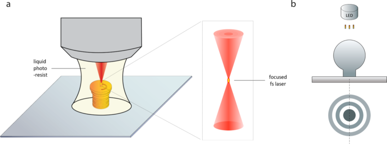
Peripheral photoinhibition (PPI) direct laser writing (DLW) is a lithography technique used to fabricate intricate 3D nanostructures that are widely employed in photonics and electronics. PPI-DLW uses two beams, one to excite the substrate and cause polymerization and the other to inhibit and quench the excitation at the edges. The capacity is limited in some systems, which can be improved through multifocal arrays. However, computing these beams is both time- and memory-intensive.
Recently, a group of researchers from Zhejiang University developed a parallel peripheral-photoinhibition lithography (P3L) system that can achieve higher efficiency nanoscale fabrication. Their work is published in Advanced Photonics
“The P3L system uses two channels, which allows the execution of different printing tasks and permits the system to fabricate highly complex structures with different periodicities,” says senior author Xu Liu.
The P3L system consists of a physical arrangement of eight modules. The system begins with two printing channels, consisting of an excitation solid spot and a doughnut-shaped inhibition beam. The two beams are first stabilized and are then split into two sub-beams using a polarization filter. This allows the individual on-off control of each sub-beam through an acoustic-optical modulator. Next, the two sub-beams are recombined to regain the excitation and inhibition beams. The beams are then modulated using spatial light modulators. Finally, the two beams are combined and passed through a microscope, after which they focus on the substrate as two spots.
The individual control of each sub-beam allows the printing of nonperiodic and complex patterns simultaneously, without compromising on scanning speed, thereby doubling the efficiency of the system. Adjusting the position and separation of the two spots is easy. These features make the proposed system more flexible and functional than conventional systems with uniform focus control.
The researchers confirmed the feasibility and potential of the system by fabricating a variety of nanostructures. They first fabricated a 2D sub-40 nm nanowire. A sub-20 nm-thick suspended nanowire was fabricated as well. After that, the researchers created two rows of alphabet patterns by printing dots, 200 nm apart. Finally, they fabricated 3D structures, including nonperiodic cubic frames, hexagonal grids, wire structures, and spherical architectures, all demonstrating exceptional resolution.
The identical on-off control of each focus increases the flexibility of the system and allows the rapid fabrication of complex, nonperiodic patterns and structures. The parallel scanning feature of the system also reduces the time cost required to fabricate large-scale, complex structures and patterns. Moreover, the new P3L system achieves a lithography efficiency that is twice that of conventional systems, regardless of whether the structure is uniform or complex.
Discussing the future potential of the work, Xu Liu says, “Multifocus parallel scanning and PPI have the ability to overcome the current challenges in DLW optical fabrication and enhance the fabrication of blazed gratings, microlens arrays, microfluidic structures, and metasurfaces. The proposed system could, furthermore, facilitate the realization of portable, high-resolution, high-throughput DLW.”
Based on these results, it is clear that the proposed P3L system will serve as a useful tool for the development of a wide range of fields that use nanotechnology.
More information:
Dazhao Zhu et al, Direct laser writing breaking diffraction barrier based on two-focus parallel peripheral-photoinhibition lithography, Advanced Photonics (2022). DOI: 10.1117/1.AP.4.6.066002
Citation:
Research team develops direct laser writing system for high-resolution, high-efficiency nanofabrication (2022, December 19)