How will materials behave under certain conditions? And how to make materials more robust? These two questions are crucial to design advanced materials for structural and functional components and applications. A close look at the underlying atomic structures and especially their defects is necessary to understand and predict material behavior.
Electrical conductivity, strength and fracture resistance are for example influenced by grain boundaries. It is known that grain boundaries—despite being defects—have their own ordered atomic structures, which can influence or even dominate material properties. However, their experimental observation requires precise and time-consuming atomic resolution imaging and is limited to the investigation of specific, individual cases.
But are these cases generalizable for all metals? A researcher team of the Max-Planck-Institut für Eisenforschung (MPIE) utilized computer simulations to show that the same atomic arrangements occur in a whole group of metals, namely fcc metals, thus proving that the “special cases” investigated in the experiments are not really exotic, but common.
This means that many previous findings are likely universal and can be adapted quickly to different materials saving time and costs of repeated experiments. The researchers now published their results in the journal Physical Review B, where their article was selected as an Editor’s Choice.
Rules for occurrence of atomic structures investigated by simulations
Material properties are mainly influenced by the underlying microstructure and its defects. Through manipulating these defects, so-called “defect engineering,” scientists will be able to improve the bulk properties of a material.
The frontier of research has expanded from understanding these defects on the micron scale towards understanding structure at the smallest scales, namely the ordering of atoms inside the different defects. This makes experiments challenging. Atomic structures can be resolved at very high resolutions, but then sample sizes become very small and the number of samples is limited.
Alternatively, macroscopic samples are used, but the structure of the defects inside them remains unknown. If, for instance, interesting phenomena can be detected at a single grain boundary, how do we know if all the grain boundaries in a sample exhibit similar structure or behavior?
“That’s the role of our simulations. We already know from experimental observations that some grain boundaries in some materials show certain ordered atomic structures that are either stable or metastable. Our question was whether there is a rule for the occurrence of these atomic structures and their thermodynamic properties in all metals,” says Dr. Tobias Brink, leader of the group Atomistic Modelling of Material Interfaces and first author of the publication.
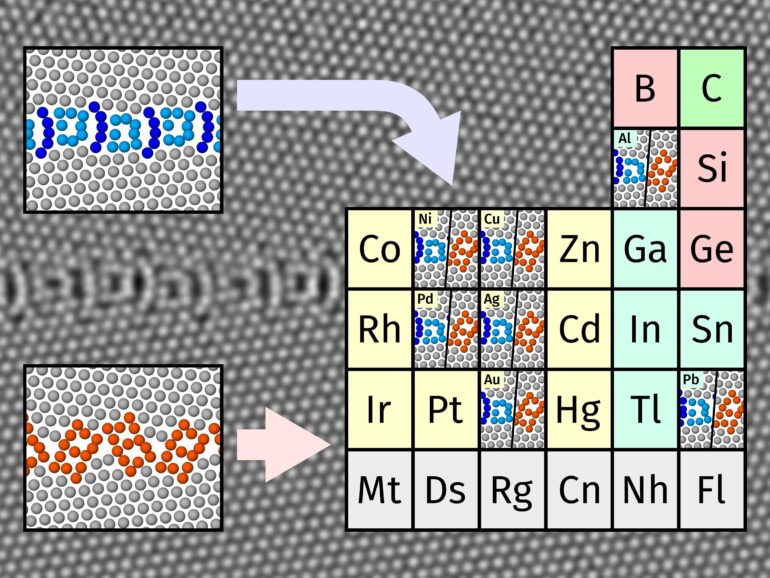
The researcher team used atomistic simulations with classical interatomic potentials in a high-throughput approach on the fcc metals nickel, copper, palladium, silver, gold, aluminum, and lead. They found two families of grain boundary structures for special grain boundary geometries.
These two families occur in all the fcc metals and can be differentiated through their densities and atomic arrangements. The scientists were also able to show that those structures arise even when using heavily simplified models that do not include realistic bonding physics, indicating that the structures are the result of the geometry of the atomic arrangements. The thermodynamic stability, however, remains specific to the material.
The researchers are now aiming to extend their findings to alloys instead of pure metals. This makes simulations and experiments more complex, but is at the same time a necessary step towards understanding and tuning materials in real life components, which are often tailored to their application by alloying.
More information:
Tobias Brink et al, Universality of grain boundary phases in fcc metals: Case study on high-angle [111] symmetric tilt grain boundaries, Physical Review B (2023). DOI: 10.1103/PhysRevB.107.054103
Provided by
Max Planck Society
Citation:
Towards defect engineering: Identifying universal structures on the atomic scale (2023, February 15)