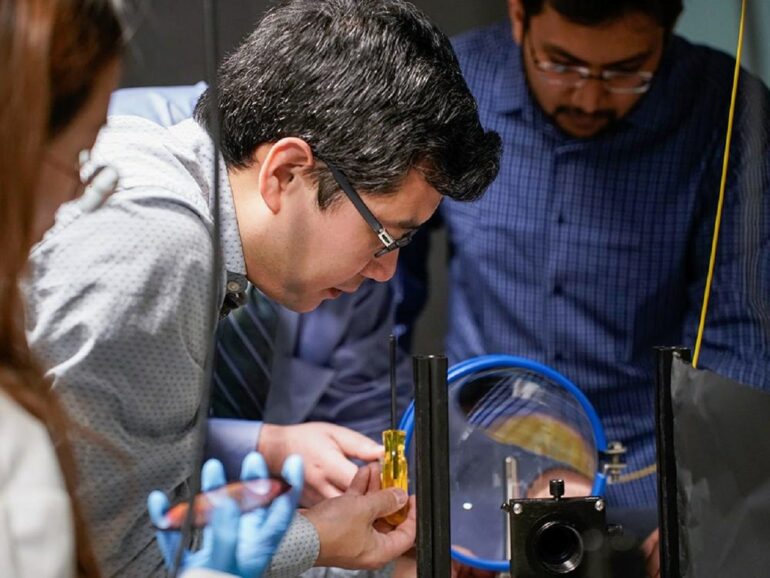
Astronomers and amateurs alike know the bigger the telescope, the more powerful the imaging capability. To keep the power but streamline one of the bulkier components, a Penn State-led research team created the first ultrathin, compact metalens telescope capable of imaging far-away objects, including the moon.
Metalenses comprise tiny, antenna-like surface patterns that can focus light to magnify distant objects in the same way as traditional curved glass lenses, but they have the advantage of being flat. Though small, millimeters-wide metalenses have been developed in the past, the researchers scaled the size of the lens to eight centimeters in diameter, or about four inches wide, making it possible to use in large optical systems, such as telescopes. They published their approach in Nano Letters.
“Traditional camera or telescope lenses have a curved surface of varying thickness, where you have a bump in the middle and thinner edges, which causes the lens to be bulky and heavy,” said corresponding author Xingjie Ni, associate professor of electrical engineering and computer science at Penn State. “Metalenses use nano-structures on the lens instead of curvature to contour light, which allows them to lay flat.”
That is one of the reasons, Ni said, modern cell-phone camera lenses protrude from the body of the phone: the thickness of the lenses take up space, though they appear flat since they are hidden behind a glass window.
Metalenses are typically made using electron beam lithography, which involves scanning a focused beam of electrons onto a piece of glass, or other transparent substrate, to create antenna-like patterns point by point. However, the scanning process of the electron beam limits the size of the lens that can be created, as scanning each point is time-consuming and has low throughput.
To create a bigger lens, the researchers adapted a fabrication method known as deep ultraviolet (DUV) photolithography, which is commonly used to produce computer chips.
“DUV photolithography is a high-throughput and high-yield process that can produce many computer chips within seconds,” Ni said. “We found this to be a good fabrication method for metalenses because it allows for much larger pattern sizes while still maintaining small details, which allows the lens to work effectively.”
The researchers modified the method with their own novel procedure, called rotating wafer and stitching. Researchers divided the wafer, on which the metalens was fabricated, into four quadrants, which were further divided into 22 by 22 millimeter regions—smaller than a standard postage stamp. Using a DUV lithography machine at Cornell University, they projected a pattern onto one quadrant through projection lenses, which they then rotated by 90 degrees and projected again. They repeated the rotation until all four quadrants were patterned.
“The process is cost-effective because the masks containing the pattern data for each quadrant can be reused due to the rotation symmetry of the metalens,” Ni said. “This reduces the manufacturing and environmental costs of the method.”
As the size of the metalens increased, the digital files required to process the patterns became significantly larger, which would take a long time for the DUV lithography machine to process. To overcome this issue, the researchers compressed the files using data approximations and by referencing non-unique data.
“We utilized every possible method to reduce the file size,” Ni said. “We identified identical data points and referenced existing ones, gradually reducing the data until we had a usable file to send to the machine for creating the metalens.”
Using the new fabrication method, the researchers developed a single-lens telescope and captured clear images of the lunar surface—achieving greater resolution of objects and much farther imaging distance than previous metalenses. Before the technology can be applied to modern cameras, however, researchers must address the issue of chromatic aberration, which causes image distortion and blurriness when different colors of light, which bend in different directions, enter a lens.
“We are exploring smaller and more sophisticated designs in the visible range, and will compensate for various optical aberrations, including chromatic aberration,” Ni said.
More information:
Lidan Zhang et al, High-Efficiency, 80 mm Aperture Metalens Telescope, Nano Letters (2022). DOI: 10.1021/acs.nanolett.2c03561
Provided by
Pennsylvania State University
Citation:
Flat, pancake-sized metalens images lunar surface in an engineering first (2023, March 3)