Computers, despite all their apparent complexity, are basically just a large number of electronic switches, flicking on and off in the right order to process digital information. Semiconductor technology has made these switches very small and incredibly fast.
The semiconducting material gallium nitride holds promise to make them even faster. This is because the charge carriers in gallium nitride, such as electrons, can move through the material at high speed. This makes GaN useful in so-called high electron-mobility transistors, or HEMTs, for high-frequency and high-power applications, including mobile phone chargers, 5G base stations, radar and satellite communications.
A crucial aspect for optimizing the operation of a HEMT is making the electrical connection that switches the transistor on or off. These so-called Schottky gates can suffer from high leakage currents that flow even when the transistor is in its off state. This results in high power consumption and limits the voltage that can be applied before the device breaks down.
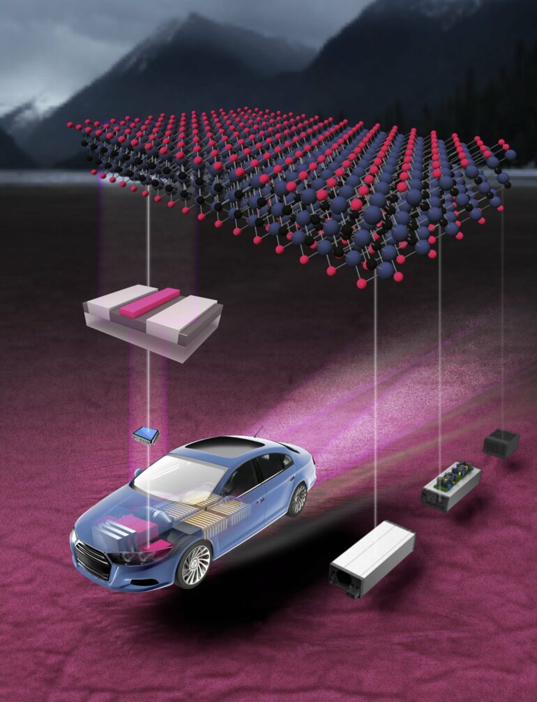
Chuanju Wang from Xiaohang Li’s team and Xiangming Xu from Husam Alshareef’s team, along with their co-workers and colleagues from India and China, have shown that these limitations can be minimized by fabricating the Schottky gate from a class of material known as MXenes: metallic two-dimensional atomically thin layers of transition metal carbides, nitrides or carbonitrides. The findings are published in the journal Advanced Materials.
While conventional metals are the traditional choice for electrical contacts to GaN, chemical interactions between the two materials create defects that can trap electrical charge and significantly limit gate controllability. “The traditional metal gate contact materials have been deposited using methods such as electron-beam evaporation and sputtering, which have a direct chemical bond with the semiconductor substrate,” explains Wang.
“We showed that our two-dimensional MXene makes a so-called van der Waals contact with the semiconductor substrate, which can significantly reduce the interface traps and fixed charges,” he says.
The KAUST team created a GaN HEMT with a gate contact made of ultraclean films of the MXene Ti3C2Tx. Their device exhibited an off-state current of just 10−7 milliamps per millimeter, which is roughly 1013 smaller than the current when the HEMT is “on.” This on–off ratio is a six-order magnitude improvement over devices with the more conventional nickel–gold contact.
“The next step is to use MXenes as the Schottky-gate contact material in other kinds of transistors, such as Ga2O3, In2O3, NiO and AlN,” says Wang.
Alshareef says that he and Professor Li are very proud of Chuanju and Xiangming for their creativity and hard work. “They deserve much of the credit for the success of this project.”
More information:
Chuanju Wang et al, Ti3C2Tx MXene van der Waals Gate Contact for GaN High Electron Mobility Transistors, Advanced Materials (2023). DOI: 10.1002/adma.202211738
Provided by
King Abdullah University of Science and Technology
Citation:
2D metal contacts stop transistor leakage currents in their tracks (2023, July 10)


