
“Margin is essentially a risk calculation, and that is a sheer impossible thing to do for a human.” explains Aart de Geus, chief executive of chip designer software maker Synopsys. “A machine will optimize everything. Everything.”
Artificial intelligence is increasingly being utilized in the design of semiconductors, and one of its advantages is that AI technology will explore design trade offs that humans would refuse to even consider.
Consider the concept of margin, for example. Designers will leave a margin for error when they place circuits on a chip, to anticipate errors in manufacturing that could, for example, throw off the timing of a signal making its way around the chip. A human wants to leave as little margin for error as possible. A machine will be bolder.
“Margin is essentially a risk calculation, and that is a sheer impossible thing to do for a human,” explains Aart de Geus, chief executive of chip designer software maker Synopsys.
“A machine will optimize everything, everything.”
De Geus spoke with ZDNet in advance of a keynote address he is giving Monday at the annual Hot Chips computer chip conference for advanced computing. The conference is being held virtually this year.
Also: AI on the bench: Cadence offers machine learning to smooth chip design
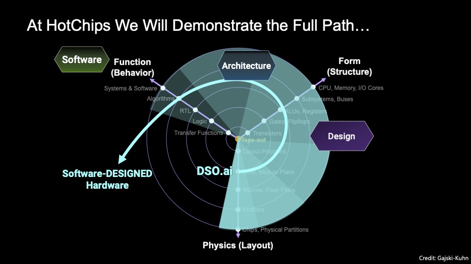
De Geus was explaining to ZDNet an expansion of AI technology in the company’s software that has been several years in the making.
The program, called DSO.ai, was first introduced a year ago in May. That program was originally able to optimize the layout of circuits in the floor plan of the chip, the way that the two-dimensional area is used.
The subject of de Geus’s keynote talk on Monday is how Synopsys is expanding beyond the physical layout optimization of a chip to optimize other factors.
One is what’s called the architecture. A chip architecture refers to what kinds of circuits and what kinds of functional blocks should be used on the chip, such as arithmetic logic units, caches, registers and pipelines.
“Fairly recently, we moved now to the beginning of micro-architectural decisions, and so for example we can now optimize also the floor plan, and the clocking scheme,” said de Geus.
In addition to physical circuit layout and architectural decisions, Synopsys is now working on a third vector for optimization, what’s called the functional aspect, or behavior, of the chip.
Also: Future of chip making to lean heavily on AI for spotting defects, says Applied Materials
That includes developing a kind of feedback loop where the software that will ultimately be run by the chip is modeled as a variable against which to optimize the logical and physical design.
“A breakthrough that I frankly thought was not going to be easily doable is that we now have also an ability to look at the software that’s going to run on the chip, do an analysis of the expected spikes of utilization, the hot power moments, and optimize the chip against that,” explained de Geus.
The ultimate goal is to set some imperatives for the chip-design program and let it figure all the stuff out on its own.
“Start with the specs of the chip, make some architectural decisions, we automate all the rest,” is how de Geus likes to describe the vision.
In initial use of the three vectors, de Geus said that Synopsys has seen a “hyper-scaler chip,” the kind of thing that would be used in a data center for massive kinds of compute — including AI — that was able to have its power consumption reduced by 27%.
“The power was reduced, but now when you can reach into the software, you are in a different league, because power reduction has always been difficult, but it is so extremely challenging to estimate it,” said de Geus. Chips are like a faucet: when they are idle, they can have little drips, leakage power, which is a relatively steady thing to measure, he said. But the dynamic power, akin to turning on and off a faucet, has far less predictability.
“Power is, in my opinion, the single most difficult physical characteristic of anything we do,” said de Geus. “Because it literally goes from the very nature of the materials used in manufacturing, the configuration of a single transistor, and so on, all the way to the application domain.”
Samsung is the first Synopsys customer to say that they have fabricated a chip that was optimized with the DSO.ai software.
Synopsys’s tool relies on a form of machine learning known as reinforcement learning. That technology was used by Google’s DeepMind unit to great effect to achieve the Alpha Zero program that beat all human players in 2016 at the games of Go and chess.
In the past two years, Google has extended machine learning to chip design automation, but only in the realm of the first vector mentioned, the physical layout. “Google is looking at the placement part, what we are optimizing for is not placement but synthesis and timing and physical and test optimization,” said de Geus. “The complexity is very large” in chip design, he emphasized, leaving lots of room to expore optimizations.

Such automation via machine learning is spreading to all participants in semiconductors. Cadence Design, Synopsys’s arch-rival, has discussed how its Cerebrus tool can bring improvements of 20% or more to chip performance, power consumption and area utilization.
And Applied Materials, the world’s biggest manufacturer of semiconductor manufacturing tools by revenue, this year unveiled SEMVision, a defect-inspection software program that uses machine learning to classify kinds of defects on a silicon wafer in a way that adjusts to new information.
To de Geus, the spread of AI throughout the tool chain of chip design is a natural consequence of AI’s spread throughout the world. In a kind of giant feedback loop, the proliferation of data, made possible by faster chips, is speeding up the activity of using those chips to analyze everything, which in turn creates greater demand for speed, putting further pressure chip makers to improve performance.
“I’ve always felt Moore’s Law was the ultimate up-push — suddenly you can do stuff you couldn’t do before,” observed de Geus. “Now, people are saying, I’m doing a little machine learning, which is great, but why are your chips so dog-slow!”
The result, he said, is “Now this mountain [of Moore’s Law] is complemented by the opposite, which is this funnel down — a technology push to an -onomic pull,” he said, referring to the economic pull of people wanting to do more to improve business outcomes.
Pressured by the push and pull, AI could be the way to find novel solutions to break the bottleneck, just as Alpha Zero found solutions that humans never saw in chess despite the rules being evident for thousands of years.
“To me they’re not surprising, but to me they’re interesting,” said de Geus of the AI approach to design.
“When you optimize everything, you reduce margin in everything,” explained de Geus. “Except, there are plenty of places on the chip where you can actually increase margin, and that statistically makes your yield higher.”
Yield means how many good chips can be gotten from a single silicon wafer, the essential economic question for all chip makers and their suppliers such as Taiwan Semiconductor Manufacturing.
A greater margin of error is an allowance for greater risk, but risk is, again, something humans find hard and often unacceptable.
That includes “risks where they [humans] don’t know what the dependencies are to the other parts of the design,” said de Geus.