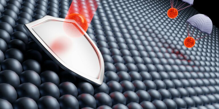
Damage from adding electrical contacts to sensitive semiconductors can be mitigated using a buffer layer and optimized deposition.
Crucial in the design of any semiconductor device is how to inject and extract an electrical current, and now a KAUST-led team has reviewed ways to do this without damage to the device.
A basic metal-semiconductor interface can create a potential energy barrier to the efficient flow of electrons, depending on the electronic properties of the two materials. It is vital to make a careful choice of contact material and the process by which this material is deposited onto the semiconductor. These design considerations are more complicated for optoelectronic components such as light-emitting diodes (LEDs), photodetectors and solar cells because these devices require a transparent contact material to allow light in or out.
Erkan Aydin and Stefaan De Wolf from the KAUST Solar Center, along with co-authors from Turkey, the Netherlands and Spain, have presented an overview for the process to stop damage occurring on devices during the creation of transparent electrodes, particularly for a technique known as sputtering.
Sputtering works by placing the target semiconductor into a vacuum chamber and surrounding it in a plasma. When an electric field is created between the target and the cathode made of the material to be sputtered, the fast-moving plasma ions transfer atoms/molecules from one to the other.
This technique is particularly useful for creating low resistivity and high transparency thin films of transparent conductive oxides (TCO), such as indium tin oxide (ITO).
However, the high kinetic energy of the ions can damage the semiconductor target. This degradation is severe enough to be seen using optical and electron microscopes, and leads to, for example, poorer device operation, lower maximum power output in solar cells and higher leakage current in LEDs.
“This is a common problem for many optoelectronic devices, but there is no universalized solution to mitigate it,” says Aydin.
Aydin and colleagues reviewed strategies for mitigating this damage, in particular using a buffer layer between the semiconductor and the electrode. “As a rule of thumb, buffer layers should be able to tolerate the particle damage during the sputtering process, while also functioning electronically and being optically transparent,” explains Aydin.
The co-authors summarize the strengths and weaknesses of different buffer materials and their suitability for different optoelectronic applications. They also compare numerous techniques for creating the buffer and give an overview for developing damage-free deposition of TCOs on optoelectronic devices in future.
“With this comprehensive review, we elaborate the problem from multiple aspects and give the readers a basic understanding of the issue and offer some cross-disciplinary learnings,” says Aydin.
More information:
Erkan Aydin et al, Sputtered transparent electrodes for optoelectronic devices: Induced damage and mitigation strategies, Matter (2021). DOI: 10.1016/j.matt.2021.09.021
Provided by
King Abdullah University of Science and Technology
Citation:
Mitigating damage caused by adding electrical contacts to sensitive semiconductors (2021, November 30)