To realize artificial intelligence systems and autonomous driving systems, processors must be able to handle more data. However, silicon-based logic devices have limitations in that processing costs and power consumption increase as miniaturization and integration progress.
To overcome these limitations, researchers are studying electronic and logic devices based on thin, two-dimensional semiconductors at an atomic layer level. However, it is more difficult to control the electrical properties through doping in two-dimensional semiconductors than in conventional silicon-based semiconductor devices. Thus, it has been technically difficult to implement logic devices with two-dimensional semiconductors.
The (KIST; President: Seok-jin Yoon) announced that a joint research team at the Korea Institute of Science and Technology, led by Dr. Do Kyung Hwang of the Center for Opto-Electronic Materials and Devices and Professor Kimoon Lee of the Department of Physics at Kunsan National University, has implemented two-dimensional, semiconductor-based electronic and logic devices with electrical properties that can be controlled via a new ultra-thin electrode material (Cl-SnSe2).
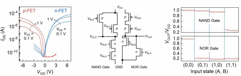
It was difficult to implement complementary logic circuits with conventional two-dimensional semiconductor devices because they only exhibit the characteristics of either N-type or P-type devices due to the Fermi-level pinning phenomenon. In contrast, the new electrode material makes it possible to freely control the characteristics of the N-type and P-type devices by minimizing defects with the semiconductor interface. In other words, a single device performs the functions of both N-type and P-type devices. Hence, there is no need to manufacture the N-type and P-type devices separately. By using this device, the joint research team successfully implemented a high-performance, low-power, complementary logic circuit that can perform logic operations such as NOR and NAND.
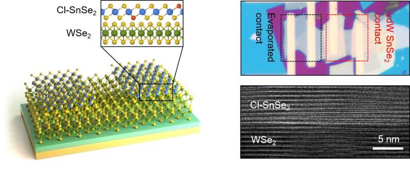
Structure of the two-dimensional semiconductor electronic device implemented in this study (left) and its image captured through an electron microscope (right). © Korea Institute of Science and Technology (KIST)
Dr. Hwang said, “This development will contribute to accelerating the commercialization of next-generation system technologies such as artificial intelligence systems, which have been difficult to use in practical applications due to technical limitations caused by the miniaturization and high integration of conventional silicon semiconductor devices. The developed two-dimensional electrode material is very thin; hence, it exhibits high light transmittance and flexibility. Therefore, it can be used for next-generation flexible and transparent semiconductor devices.”
The study is published in Advanced Materials.
More information:
Jisu Jang et al, Fermi‐Level Pinning‐Free WSe 2 Transistors via 2D Van der Waals Metal Contacts and Their Circuits, Advanced Materials (2022). DOI: 10.1002/adma.202109899
Provided by
National Research Council of Science & Technology
Citation:
New ultra-thin electrode material gets us a step closer to next-generation semiconductors (2022, May 30)