To make the top-of-the-line chips for Apple’s iPhone, such as the A14, or Nvidia’s A100 series AI processors, with billions of transistors, it takes a factory that costs $16 billion to build and maintain. That amount is up from $10 billion just eight years ago, and is set to rise significantly again, to perhaps $18 billion in the next few years.
That has presented the chip industry with a quandary: Such chips more than ever need to be checked for defects, but chip makers are under more pressure than ever to get product out the door to recoup their investment.
“You should naturally want to inspect more, because there are more process steps, more things that can go wrong, but if you look at what has happened, the economics have prohibited our customers from doing that inspection,” said Keith Wells, who is group vice president of the imaging and process control group at Applied Materials, the biggest maker of tools for making chips.
“We see this need to really solve this economic problem for our customers,” said Wells, who spoke with ZDNet via Zoom.
A number of tools are being employed to solve that economic quandary, and one of the areas with the most potential, said Wells, is artificial intelligence, in particular the machine learning form of AI.

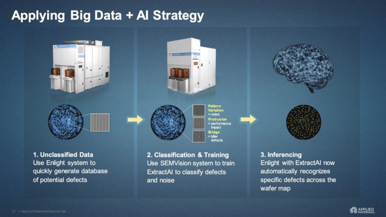
An optical scanner, Enlight, does a quick read of a chip wafer, at low resolution, calling out what may be defects. A scanning electron microscope, SEMVision, does a slower scan of only sections of the wafer, carefully classifying suspected defects as benign anomalies or serious defects. A machine learning classifer, ExtractAI, uses the output of SEMVision to identify more areas as worthy of closer review, and directs the SEMVision to take a look.
Applied Materials
In March, the company unveiled Enlight, a scanner that was five years in development and that was deployed in beta in 2019.
Enlight uses light polarization to maximize resolution and to find critical defects in half the time of the typical optical scanner. The scanner for the first time will capture both direct light bouncing off the wafer surface, and scattered light, known as “brightfield” and “greyfield,” respectively. That’s like scanning two things in one pass, cutting in half the time required.
In addition to the new optics, however, the scanner will take algorithms that are variable, rather than being hardwired. That opens the way to algorithms for learned functions using machine learning.
With more and more particles appearing on wafers, chip makers have to sort out what particles will actually be fatal to a chip. Examples of defects that are really bad are an “open,” where a circuit is broken apart, or “short,” where two circuits parallel to one another have been bridged by a particle that’s fallen between them.
That leads to a classification problem that’s a classic machine learning task: Is this defect fatal, or manageable?
“When you get down to 5 nanometer, if a particle falls in an open area, you don’t care, it’s not likely to impact a circuit,” explained Wells. “But if falls on top of a transistor, it’s likely to kill the die,” meaning that part of the silicon wafer is unusable. Chip making is all about how many chips can be gotten from a wafer, the known good die. That metric is the “yield” of chip making.
“Hence, our customers want to know not just what’s on the wafer, but what is or isn’t likely to kill the wafer, so you’ve got to sort between those two things,” said Wells.
That process of making a judgment is a two-part process, detecting, then classifying. One is fast, one is slow.
The Enlight scanner, by being faster than previous scanners, is able to be used more frequently during manufacturing, thereby gathering more images of potential defects. In fifteen minutes to an hour, it will generate perhaps a million images of what could be a fatal defect, or what could be just noise in the scattered light.
Those million potential defects are fed to a separate tool, called SEMVision, which does the classifying. SEMVision is a scanning electron microscope. It scans the surface of the wafer with a focused beam of electrons. It looks more slowly, at greater resolution, at just a section of the wafer that has been suggested by Enlight. It takes a look at potential defects called out by Enlight to see whether they are opens or bridges, or maybe a harmless protrusion. It classifies what it sees.
The SEMVision takes thirty minutes to scan, and then forty-five minutes to review. “These work together, detection with the optical system, and very high-resolution review with the eBeam tool,” explained Wells. “You use that for the initial training of your AI, that then tells you the prediction of the yield-killer defects.”
The data from Enlight and SEMVision will both be sent to a third system, a rack-based computer running a program called ExtractAI. The program calculates a probability of a section of wafer, and can tell SEMVision how to use its slow approach to review other areas.
“ExtractAI says, I looked at the last fifteen defects put into this n-dimensional space, and they’re all bridges, so now I am very confident on all those being bridges,” explained Wells.
“Stop looking at those areas, go sample this population and take 50 or 100 of those, and it walks through that with this backwards and forward communication between the SEMVision and the ExtractAI computer.”
That feedback loop is new in the use of AI, said Wells. The traditional use of scanning electron microscopes uses a static set of rules to classify defects.
“You hear people say we use AI, but they set up a static classifier, and then there has to be someone to decide if that classifier is no longer good, the process has changed,” explained Wells.
In contrast, “this classification scheme is constantly adapting, and updating itself,” he said of ExtractAI.
“Every wafer that goes through Enlight and is sent to SEMVision, goes to a real-time AI process that learns and adapts our classifier to figure out what is a yield-killing defect versus a nuisance. Every cycle of Enlight to SEMVision to ExtractAI “tries to optimize the output” all over again.
“We are using an adaptive learning method, which is unique,” he said. That means that “every wafer, we are adapting to what we see, every wafer the AI is making a decision and trying to optimize the result.”

The ExtractAI, once trained, can use the entire million points of interest to classify the entire wafer surface. “We give an actual defect map, and it’s more accurate and more valuable than what a competitor can do,” said Wells.
The achievement is a confluence of factors. The speed-up of optical scanning with Enlight allows for seeing more things earlier than a human looking at the output of the SEM microscope. But the computational capability that has come to faster computer algorithms has allowed for continuous re-training.
“It’s this synergistic thing happening in the semiconductor industry,” he said, “suddenly GPUs and GPUs are fast enough you can start deploying AI and getting results quickly.”
“The computational element of making this near real-time, where you have answers in a few seconds, has been a key element in the adoption of this.”
Wells would not disclose the exact details of the machine learning algorithms, citing protected intellectual property. It is not really deep learning, he made clear, given that there are fewer data points.
“It’s closer to what’s thought of as traditional machine learning than a neural net, and one reason we went down that path is that neural nets are very heavy,” said Wells.
“We have big data, but if you look at a Google image classifier, their set-up of those are hundreds of thousands of data points, whereas we have thousands of data points.”
What works well with those thousands initially, to get wafer inspection up and running, “is closer to a machine learning approach, where you extract the attributes” of interest, “and then you use techniques to figure out which attributes are most important in a classification.”
Keep in mind, the factory is a secure facility. It is not on the Internet there is no outside connection to the tool in the chip fab, noted Wells.
“When you are figuring out how to do this, you can start with an algorithm that has some weights in it, but that doesn’t contain anyone’s IP,” he said. “But then all additional data to do training can only be generated on site, in that fab, we can’t bring in a bunch of other data points.”
The immediate economic payoff of Enlight and SEMVision and ExtractAI, said Wells, is that the the combined tools are inspecting wafers 1.6 times more frequently, which leads to more chances to find the killer defect.
The ExtractAI tool has been used exclusively for logic circuits to date, and is just now being rolled out in beta to makers of DRAM and NAND memory chips, said Wells.