The electronic and optical devices that we use on a daily basis, such as mobile phones, LEDs and solar cells use transistors and other parts that are consistently getting smaller and more compact. With an ever-growing need for computing power, storage, and energy efficiency, this trend will only continue to new extremes.
Producing such small components for electronic devices requires the machining and preparation of structures on sub-micron scales, up to hundreds of times smaller than the width of a human hair. But current methods for the nanofabrication of surfaces use photolithography and e-beam lithography—methods that are complicated, extremely expensive, generally inaccessible, and require high levels of expertise.
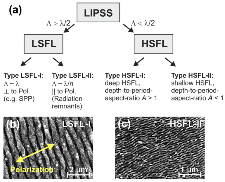
Laser-induced periodic surface structure (LIPSS) has been earmarked as a novel and prospective alternative to these methods. In LIPSS, femtosecond lasers are used to deliver ultrashort laser pulses that spontaneously lead to the formation of periodic patterns on the surface that are much smaller than the laser wavelength.
A well-known parameter in LIPSS is the choice of laser wavelength, which directly affects the periodicity of the formed structures. However other parameters have remained unstudied. The major concerns regarding the standardized use of LIPSS include the quality of the formed surface structure, namely the crystallinity of the substrate, potential for defects, and strain. To consistently produce LIPSS with controllable properties and characteristics for specific applications, it is critical to understand which laser sources should be used for which particular need.
To answer these questions in more depth, a Japanese research collaboration led by scientists from the Nagoya Institute of Technology, has now directly investigated the various parameters that are influenced by laser choice. The work, in collaboration with Osaka University, Tokai University, Kyoto University, and the Japan Atomic Energy Agency (JAEA), was led by Assistant Professor Reina Miyagawa of the Nagoya Institute of Technology, alongside Associate Professor Norimasa Ozaki of Osaka University, and Professor Masaki Hashida of Tokai University, who is also a researcher at Kyoto University. Their findings have been published in Scientific Reports.
“In our study, we chose silicon as a substrate, as it is a material used in many optoelectronic devices the world over, like transistors, mobile phones and solar cells,” explains Dr. Miyagawa.
The researchers used two different femtosecond lasers on the substrate. In one experiment, a titanium and sapphire (Ti:Sapphire) laser system with pulses of 0.8 µm was used to structure the silicon at energies higher than the band-gap energy. In the other experiment, the researchers used a free-electron laser at mid-infrared pulses of 11.4 µm, which could probe the effect at energies lower than the sample band-gap energy.
The analysis of the LIPSS samples was done both microscopically and macroscopically. The microscopic crystallinity and purity were studied using transmission electron microscopy (TEM), while a more macroscopic analysis of the strain and stability of the wider structure was investigated using synchrotron high-energy X-ray diffraction (XRD).
“When the Ti:Sapphire laser was used, the observed LIPSS retained the highly crystalline nature of the silicon but seemed to take on some residual strain. In contrast, the LIPSS which was formed by the mid-infrared free-electron laser led to some clearly visible defects. However, there was no observable strain to the system whatsoever,” adds Dr. Miyagawa.
This study constitutes the first report on the high-resolution, microscopic and macroscopic observations of crystallinity in LIPSS using synchrotron high-energy X-ray diffraction. The findings indicate how LIPSS can be tuned and tailored for specific applications by manipulating its defects, strain, and periodicity, through an appropriate choice of laser.

Continued research along these lines can open the pathway toward the widespread application of LIPSS to achieve the cost-effective, simple, and accessible fabrication of nanostructured surfaces for applications in a wide range of optoelectronic devices.
More information:
Reina Miyagawa et al, Crystallinity in periodic nanostructure surface on Si substrates induced by near- and mid-infrared femtosecond laser irradiation, Scientific Reports (2022). DOI: 10.1038/s41598-022-25365-1
Provided by
Nagoya Institute of Technology
Citation:
Investigating the laser-induced periodic surface structure (LIPSS) of silicon (2023, January 10)